


Bilder dienen nur zur Referenz. Siehe Produktspezifikationen.
Bestellungen über
$5000
74LVC1G17GW,125

Single Schmitt trigger buffer


Marken: Nexperia
Herstellerteil #: 74LVC1G17GW,125
Datenblatt: 74LVC1G17GW,125 Datenblatt (PDF)
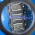
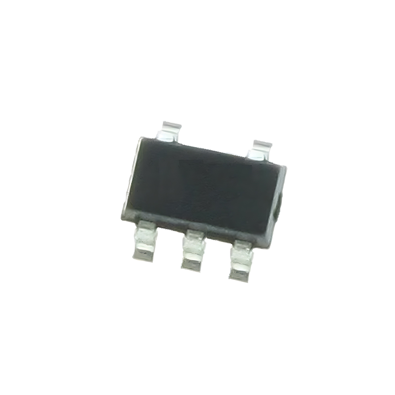
Paket/Gehäuse: TSSOP-5
RoHS-Status:
Lagerzustand: 5.414 Stück, Neues Original
Produktart: Buffers, Drivers, Receivers, Transceivers
Warranty: 1 Year Ovaga Warranty - Find Out More
0
1
*Alle Preise sind in USD
| Menge | Einzelpreis | Ext. Preis |
|---|---|---|
| 5 | $0,079 | $0,395 |
| 50 | $0,063 | $3,150 |
| 150 | $0,056 | $8,400 |
| 500 | $0,051 | $25,500 |
| 3000 | $0,045 | $135,000 |
| 6000 | $0,043 | $258,000 |
Auf Lager: 5.414 Stck
74LVC1G17GW,125 Allgemeine Beschreibung
The 74LVC1G17GW,125 is your go-to choice for voltage translation challenges in today's electronics landscape. With its ability to work with 3.3V and 5V devices, this single buffer Schmitt-trigger serves as a versatile solution for mixed-voltage environments. Its partial power down features, including I circuitry that disables the output, ensure that the device remains protected during low-power usage, preventing any potential damage from backflow current. Whether you're integrating diverse systems or navigating intricate voltage requirements, the 74LVC1G17GW,125 offers the performance and reliability necessary for success in a fast-paced technological world
Funktionen
- Wide supply voltage range from 1.65 V to 5.5 V
- Overvoltage tolerant inputs to 5.5 V
- High noise immunity
- CMOS low power dissipation
- IOFF circuitry provides partial Power-down mode operation
- ±24 mA output drive (VCC = 3.0 V)
- Latch-up performance exceeds 250 mA
- Direct interface with TTL levels
- Unlimited rise and fall times
- Complies with JEDEC standard:JESD8-7 (1.65 V to 1.95 V)JESD8-5 (2.3 V to 2.7 V)JESD8C (2.7 V to 3.6 V)JESD36 (4.5 V to 5.5 V)
- JESD8-7 (1.65 V to 1.95 V)
- JESD8-5 (2.3 V to 2.7 V)
- JESD8C (2.7 V to 3.6 V)
- JESD36 (4.5 V to 5.5 V)
- ESD protection:HBM: ANSI/ESDA/JEDEC JS-001 class 2 exceeds 2000 VCDM: ANSI/ESDA/JEDEC JS-002 class C3 exceeds 1000 V
- HBM: ANSI/ESDA/JEDEC JS-001 class 2 exceeds 2000 V
- CDM: ANSI/ESDA/JEDEC JS-002 class C3 exceeds 1000 V
- Multiple package options
- Specified from -40 °C to +85 °C and -40 °C to +125 °C
Anwendung
- Industrial
- Automation & Process Control
- Signal Processing
- Automotive
Spezifikationen
| Parameter | Wert | Parameter | Wert |
|---|---|---|---|
| Type number | 74LVC1G17GW | Product status | Production |
| VCC (V) | 1.65 - 5.5 | Logic switching levels | CMOS/LVTTL |
| Output drive capability (mA) | ± 32 | fmax (MHz) | 175 |
| Nr of bits | 1 | Power dissipation considerations | low |
| Tamb (°C) | -40~125 | Rth(j-a) (K/W) | 319 |
| Rth(j-c) (K/W) | 188 | Package name | TSSOP5 |
| Packing | SOT353-1_125 | Orderable part number | 74LVC1G17GW,125 |
| Chemical content | 74LVC1G17GW |
Versand
| Versandart | Versandgebühr | Vorlaufzeit | |
|---|---|---|---|
 |
DHL | $20.00-$40.00 (0.50 KG) | 2-5 Tage |
 |
FedEx | $20.00-$40.00 (0.50 KG) | 2-5 Tage |
 |
UPS | $20.00-$40.00 (0.50 KG) | 2-5 Tage |
 |
TNT | $20.00-$40.00 (0.50 KG) | 2-5 Tage |
 |
EMS | $20.00-$40.00 (0.50 KG) | 2-5 Tage |
 |
REGISTRIERTE LUFTPOST | $20.00-$40.00 (0.50 KG) | 2-5 Tage |
Bearbeitungszeit: Die Versandkosten hängen von der jeweiligen Zone und dem Land ab.
Zahlung
| Zahlungsbedingungen | Handgebühr | |
|---|---|---|
 |
Banküberweisung | Bankgebühr in Höhe von 30,00 USD wird berechnet. |
 |
Paypal | 4,0 % Servicegebühr wird berechnet. |
 |
Kreditkarte | 3,5 % Servicegebühr wird berechnet. |
 |
Western Union | charge US.00 banking fee. |
 |
Geldgramm | Bankgebühr in Höhe von 0,00 USD wird berechnet. |
Garantien
1. Die von Ihnen gekauften elektronischen Bauteile enthalten eine 365-tägige Garantie. Wir garantieren die Produktqualität.
2. Wenn einige der Artikel, die Sie erhalten haben, nicht von perfekter Qualität sind, würden wir verantwortungsvoll Ihre Rückerstattung oder Ersatz arrangieren. Die Artikel müssen jedoch in ihrem Originalzustand verbleiben.
Verpackung
-

Schritt1 :Produkt
-

Schritt2 :Vakuumverpackung
-

Schritt3 :Antistatikbeutel
-

Schritt4 :Individuelle Verpackung
-

Schritt5 :Verpackungskartons
-

Schritt6 :Barcode-Versandetikett


Alle Produkte werden in antistatischen Beuteln verpackt. Versand mit ESD-Antistatikschutz.
Auf dem äußeren ESD-Verpackungsetikett werden die Informationen unseres Unternehmens verwendet: Teilenummer, Marke und Menge.
Wir prüfen alle Waren vor dem Versand, stellen sicher, dass sich alle Produkte in gutem Zustand befinden und dass die Teile neu und original sind und mit dem Datenblatt übereinstimmen.
Nachdem alle Waren darauf überprüft wurden, dass nach dem Verpacken keine Probleme auftreten, werden wir sicher verpacken und per Global Express versenden. Es zeigt eine ausgezeichnete Durchstoß- und Reißfestigkeit sowie eine gute Dichtungsintegrität.


Teilpunkte
-
The 74LVC1G17GW,125 is a single buffer gate chip that features open-drain outputs. It operates at a voltage from 1.65V to 5.5V and is suitable for interfacing between different voltage domains. The chip is designed for low-power consumption and has a high-speed operation.
-
Equivalent
Some equivalent products of the 74LVC1G17GW,125 chip include the SN74LVC1G17 and the TC7WH17FK,5. These chips are also single Schmitt-trigger buffers with open-drain outputs and have similar voltage and current specifications. -
Features
Features of 74LVC1G17GW,125 include single buffer with open-drain output, wide operating voltage range of 1.65V to 5.5V, high-speed switching with 5-ns propagation delay, low-power consumption, and schmitt trigger input for noise immunity. It is available in a space-saving SOT353 package. -
Pinout
The 74LVC1G17GW,125 is a single non-inverting buffer with Schmitt-trigger input. It has a total of 6 pins, with the following functions: Pin 1 (A): Input, Pin 3 (Y): Output, Pin 5 (VCC): Power supply, Pin 6 (GND): Ground. -
Manufacturer
The manufacturer of the 74LVC1G17GW,125 is NXP Semiconductors. NXP Semiconductors is a Dutch-American semiconductor manufacturer specializing in the development and production of a wide range of products including microcontrollers, logic ICs, power management, and connectivity solutions for various industries such as automotive, industrial, mobile, and consumer electronics. -
Application Field
The 74LVC1G17GW,125 is commonly used in applications requiring buffer or signal inversion functions, such as amplifiers, level shifters, and clock signal distribution. It can also be used in portable devices, consumer electronics, industrial control systems, and automotive applications due to its low power consumption and high-speed operation. -
Package
The 74LVC1G17GW,125 chip is a Single Buffer/Driver with Open-Drain Output in a SOT-353 package. It has a form of Surface Mount and a size of 1.45mm x 1.00mm x 0.75mm.


Wir bieten qualitativ hochwertige Produkte, durchdachten Service und eine Kundendienstgarantie
-

Wir haben reichhaltige Produkte, die Ihre unterschiedlichen Bedürfnisse erfüllen können.
-

Die Mindestbestellmenge beginnt bei 1 Stück.
-

Niedrigste internationale Versandgebühr beginnt ab 0,00 USD
-

365 Tage Qualitätsgarantie für alle Produkte


