


Bilder dienen nur zur Referenz. Siehe Produktspezifikationen.
Bestellungen über
$5000Altera EP2C5T144C7N
FPGA with PLL, 89 I/O's


Marken: Altera Corporation (Intel)
Herstellerteil #: EP2C5T144C7N
Datenblatt: EP2C5T144C7N Datasheet (PDF)
Paket/Gehäuse: TQFP-144
Produktart: FPGAs (Field Programmable Gate Array)
RoHS-Status:
Lagerzustand: 3.969 Stück, Neues Original
Warranty: 1 Year Ovaga Warranty - Find Out More
0
1
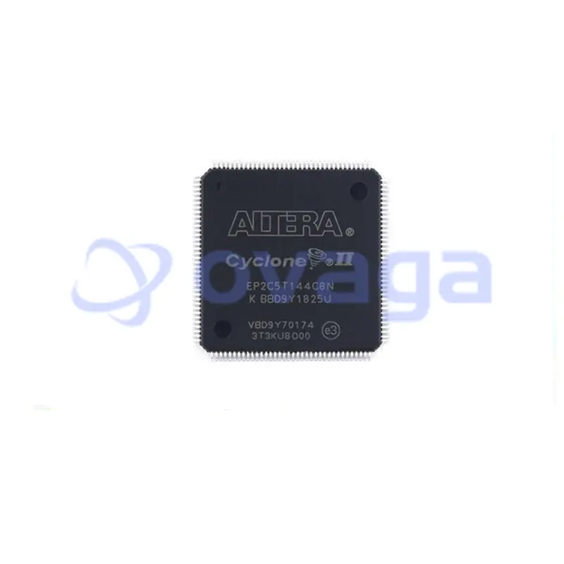
EP2C5T144C7N Allgemeine Beschreibung
The EP2C5T144C7N is a CYCLONE II FPGA featuring 5K logic elements in a compact surface mount device (SMD) package with 2C5T144 configuration. With a total of 4608 macrocells, this FPGA from the Cyclone II family offers a versatile solution for a wide range of applications. The logic case style is TQFP, with 144 pins for seamless integration into your designs
Funktionen
- 5,120 logic elements (LEs)
- 356 kilobits (Kb) of embedded memory
- 56 18x18-bit hardware multipliers
- 298 user I/O pins
- Four-phase power sequencing
- JTAG and AS programming interfaces
- On-chip PLLs (phase-locked loops) and DLLs (delay-locked loops)
Anwendung
- High-performance computing
- Video and image processing
- Industrial automation and control
- Automotive
- Communications
Spezifikationen
| Parameter | Wert | Parameter | Wert |
|---|---|---|---|
| feature-family-name | Cyclone® II | feature-process-technology | 90nm |
| feature-maximum-number-of-user-i-os | 89 | feature-number-of-registers | |
| feature-device-logic-cells | 4608 | feature-device-system-gates | |
| feature-number-of-multipliers | 13 (18x18) | feature-program-memory-type | SRAM |
| feature-ram-bits-kbit | 117 | feature-total-number-of-block-ram | 26 |
| feature-ethernet-macs | feature-supported-ip-core | Viterbi Compiler, Low-Speed/Hybrid Serial Decoder|V1 ColdFire|SpeedView Enabled JPEG Encoder (SVE-JPEG-E)|10 Gigabit Ethernet MAC|32/64-bit PCI-X bus Master/Target interface Core, 66/100/133Mhz | |
| feature-supported-ip-core-manufacture | Altera/Freescale/CAST, Inc/MorethanIP/PLDA | feature-maximum-number-of-serdes-channels | |
| feature-device-logic-units | 4608 | feature-device-number-of-dlls-plls | 2 |
| feature-transceiver-blocks | feature-transceiver-speed-gbps | ||
| feature-dedicated-dsp | feature-pci-blocks | ||
| feature-programmability | No | feature-maximum-internal-frequency-mhz | 402.58 |
| feature-speed-grade | 7 | feature-giga-multiply-accumulates-per-second | |
| feature-differential-i-o-standards-supported | LVDS|PCI-X | feature-single-ended-i-o-standards-supported | LVDS|PCI-X |
| feature-external-memory-interface | DDR SDRAM|QDR II+SRAM | feature-minimum-operating-supply-voltage-v | 1.15 |
| feature-maximum-operating-supply-voltage-v | 1.25 | feature-packaging | |
| feature-rohs | feature-rad-hard | ||
| feature-pin-count | 144 | feature-supplier-package | TQFP |
| feature-standard-package-name1 | QFP | feature-cecc-qualified | No |
| feature-esd-protection | feature-escc-qualified | ||
| feature-military | No | feature-aec-qualified | No |
| feature-aec-qualified-number | feature-auto-motive | No | |
| feature-p-pap | No | feature-eccn-code | EAR99 |
| feature-svhc | No |
Versand
| Versandart | Versandgebühr | Vorlaufzeit | |
|---|---|---|---|
 |
DHL | $20.00-$40.00 (0.50 KG) | 2-5 Tage |
 |
FedEx | $20.00-$40.00 (0.50 KG) | 2-5 Tage |
 |
UPS | $20.00-$40.00 (0.50 KG) | 2-5 Tage |
 |
TNT | $20.00-$40.00 (0.50 KG) | 2-5 Tage |
 |
EMS | $20.00-$40.00 (0.50 KG) | 2-5 Tage |
 |
REGISTRIERTE LUFTPOST | $20.00-$40.00 (0.50 KG) | 2-5 Tage |
Bearbeitungszeit: Die Versandkosten hängen von der jeweiligen Zone und dem Land ab.
Zahlung
| Zahlungsbedingungen | Handgebühr | |
|---|---|---|
 |
Banküberweisung | Bankgebühr in Höhe von 30,00 USD wird berechnet. |
 |
Paypal | 4,0 % Servicegebühr wird berechnet. |
 |
Kreditkarte | 3,5 % Servicegebühr wird berechnet. |
 |
Western Union | charge US.00 banking fee. |
 |
Geldgramm | Bankgebühr in Höhe von 0,00 USD wird berechnet. |
Garantien
1. Die von Ihnen gekauften elektronischen Bauteile enthalten eine 365-tägige Garantie. Wir garantieren die Produktqualität.
2. Wenn einige der Artikel, die Sie erhalten haben, nicht von perfekter Qualität sind, würden wir verantwortungsvoll Ihre Rückerstattung oder Ersatz arrangieren. Die Artikel müssen jedoch in ihrem Originalzustand verbleiben.
Verpackung
-

Schritt1 :Produkt
-

Schritt2 :Vakuumverpackung
-

Schritt3 :Antistatikbeutel
-

Schritt4 :Individuelle Verpackung
-

Schritt5 :Verpackungskartons
-

Schritt6 :Barcode-Versandetikett


Alle Produkte werden in antistatischen Beuteln verpackt. Versand mit ESD-Antistatikschutz.
Auf dem äußeren ESD-Verpackungsetikett werden die Informationen unseres Unternehmens verwendet: Teilenummer, Marke und Menge.
Wir prüfen alle Waren vor dem Versand, stellen sicher, dass sich alle Produkte in gutem Zustand befinden und dass die Teile neu und original sind und mit dem Datenblatt übereinstimmen.
Nachdem alle Waren darauf überprüft wurden, dass nach dem Verpacken keine Probleme auftreten, werden wir sicher verpacken und per Global Express versenden. Es zeigt eine ausgezeichnete Durchstoß- und Reißfestigkeit sowie eine gute Dichtungsintegrität.


Teilpunkte
-
The EP2C5T144C7N chip is a field-programmable gate array (FPGA) designed by Altera (now Intel). It belongs to the Cyclone II series and contains 5,136 logic elements and 36,864 bits of embedded memory. The chip has 144 pins and is commonly used in applications requiring high-performance digital signal processing, embedded processing, and high-speed communication. It offers significant flexibility and can be reprogrammed to perform different functions.
-
Equivalent
Some equivalent products of EP2C5T144C7N chip are EP2C5T144I7N, EP2C5Q208C7N, and EP2C5Q208I7N. -
Features
The EP2C5T144C7N is a Cyclone II FPGA that features 5,136 logic elements, 9 embedded multipliers, and 288 Kbits of on-chip RAM. It operates at a maximum frequency of 250 MHz and offers 1 industry-standard 10/100 Ethernet MAC PHY interface. The FPGA is housed in a 144-pin TQFP package. -
Pinout
The EP2C5T144C7N has a pin count of 144. It is an FPGA (Field Programmable Gate Array) which can be reprogrammed to perform various functions in digital circuits. -
Manufacturer
Altera Corporation is the manufacturer of the EP2C5T144C7N. It is a semiconductor company specializing in programmable logic devices, including field-programmable gate arrays (FPGAs) and complex programmable logic devices (CPLDs). Altera provides high-performance solutions for various industries such as telecommunications, automotive, industrial automation, and aerospace. -
Application Field
The EP2C5T144C7N is a small and low-cost field-programmable gate array (FPGA) that can be used in various applications such as industrial automation, robotics, telecommunications, data processing, and embedded systems. It offers flexible and reprogrammable logic and is suitable for prototyping and development of complex digital systems. -
Package
The EP2C5T144C7N chip has a package type of TQFP, a form of 144-terminal, and a size of 14mm x 14mm.


Datenblatt PDF
Wir bieten qualitativ hochwertige Produkte, durchdachten Service und eine Kundendienstgarantie
-

Wir haben reichhaltige Produkte, die Ihre unterschiedlichen Bedürfnisse erfüllen können.
-

Die Mindestbestellmenge beginnt bei 1 Stück.
-

Niedrigste internationale Versandgebühr beginnt ab 0,00 USD
-

365 Tage Qualitätsgarantie für alle Produkte


