Bilder dienen nur zur Referenz. Siehe Produktspezifikationen.
Bestellungen über
$5000EP2S180F1020C3
With its Field Programmable Gate Array technology, the EP2S180F1020C3 offers customizable solutions for complex designs


Marken: ALTERA CORP
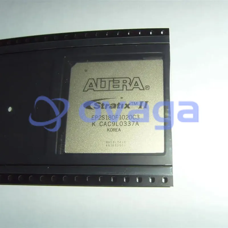
Herstellerteil #: EP2S180F1020C3
Datenblatt: EP2S180F1020C3 Datenblatt (PDF)
Paket/Gehäuse: FBGA-1020
Produktart: FPGAs (Field Programmable Gate Array)
RoHS-Status:
Lagerzustand: 6.554 Stück, Neues Original
Warranty: 1 Year Ovaga Warranty - Find Out More
0
1
EP2S180F1020C3 Allgemeine Beschreibung
Boasting a 180,000 logic element capacity and a C3 speed grade, the EP2S180F1020C3 is a formidable Altera Stratix II FPGA designed for high-performance processing. With 1,020 pins and a wide range of I/O options, this FPGA is equipped to handle complex logic functions, high-speed data processing, and real-time signal processing across various industries. Its support for embedded memory blocks, high-speed transceivers, and flexible routing resources ensures that it can meet the demanding requirements of modern applications
Funktionen
- The Stratix II family offers the following
- features:
- 15,600 to 179,400 equivalent LEs; see Table 1–1
- New and innovative adaptive logic module (ALM), the basic building block of the Stratix II architecture, maximizes performance and resource usage efficiency
- Up to 9,383,040 RAM bits (1,172,880 bytes) available without reducing logic resources
- TriMatrix memory consisting of three RAM block sizes to implement true dual-port memory and first-in first-out (FIFO) buffers
- High-speed DSP blocks provide dedicated implementation of multipliers (at up to 450 MHz), multiply-accumulate functions, and finite impulse response (FIR) filters
- Up to 16 global clocks with 24 clocking resources per device region
- Clock control blocks support dynamic clock network enable/disable, which allows clock networks to power down to reduce power consumption in user mode
- Up to 12 PLLs (four enhanced PLLs and eight fast PLLs) per device provide spread spectrum, programmable bandwidth, clock switchover, real-time PLL reconfiguration, and advanced multiplication and phase shifting
- Support for numerous single-ended and differential I/O standards
- High-speed differential I/O support with DPA circuitry for 1-Gbps performance
- Support for high-speed networking and communications bus standards including Parallel RapidIO, SPI-4 Phase 2 (POS-PHY Level 4), HyperTransport™ technology, and SFI-4
- Support for high-speed external memory, including DDR and DDR2 SDRAM, RLDRAM II, QDR II SRAM, and SDR SDRAM
- Support for multiple intellectual property megafunctions from Altera MegaCore® functions and Altera Megafunction Partners Program (AMPPSM) megafunctions
- Support for design security using configuration bitstream encryption
- Support for remote configuration updates
Spezifikationen
| Parameter | Wert | Parameter | Wert |
|---|---|---|---|
| Pbfree Code | No | Rohs Code | No |
| Part Life Cycle Code | Transferred | Ihs Manufacturer | ALTERA CORP |
| Part Package Code | BGA | Package Description | 33 X 33 MM, 1 MM PITCH, FBGA-1020 |
| Pin Count | 1020 | Reach Compliance Code | not_compliant |
| HTS Code | 8542.39.00.01 | Clock Frequency-Max | 717 MHz |
| Combinatorial Delay of a CLB-Max | 4.672 ns | JESD-30 Code | S-PBGA-B1020 |
| JESD-609 Code | e0 | Length | 33 mm |
| Moisture Sensitivity Level | 4 | Number of CLBs | 71760 |
| Number of Inputs | 742 | Number of Logic Cells | 179400 |
| Number of Outputs | 734 | Number of Terminals | 1020 |
| Operating Temperature-Max | 85 °C | Operating Temperature-Min | |
| Organization | 71760 CLBS | Package Body Material | PLASTIC/EPOXY |
| Package Code | BGA | Package Equivalence Code | BGA1020,32X32,40 |
| Package Shape | SQUARE | Package Style | GRID ARRAY |
| Peak Reflow Temperature (Cel) | 220 | Power Supplies | 1.2,1.5/3.3,3.3 V |
| Programmable Logic Type | FIELD PROGRAMMABLE GATE ARRAY | Qualification Status | Not Qualified |
| Seated Height-Max | 3.5 mm | Supply Voltage-Max | 1.25 V |
| Supply Voltage-Min | 1.15 V | Supply Voltage-Nom | 1.2 V |
| Surface Mount | YES | Technology | CMOS |
| Temperature Grade | OTHER | Terminal Finish | TIN LEAD |
| Terminal Form | BALL | Terminal Pitch | 1 mm |
| Terminal Position | BOTTOM | Time@Peak Reflow Temperature-Max (s) | 20 |
| Width | 33 mm |
Versand
| Versandart | Versandgebühr | Vorlaufzeit | |
|---|---|---|---|
 |
DHL | $20.00-$40.00 (0.50 KG) | 2-5 Tage |
 |
FedEx | $20.00-$40.00 (0.50 KG) | 2-5 Tage |
 |
UPS | $20.00-$40.00 (0.50 KG) | 2-5 Tage |
 |
TNT | $20.00-$40.00 (0.50 KG) | 2-5 Tage |
 |
EMS | $20.00-$40.00 (0.50 KG) | 2-5 Tage |
 |
REGISTRIERTE LUFTPOST | $20.00-$40.00 (0.50 KG) | 2-5 Tage |
Bearbeitungszeit: Die Versandkosten hängen von der jeweiligen Zone und dem Land ab.
Zahlung
| Zahlungsbedingungen | Handgebühr | |
|---|---|---|
 |
Banküberweisung | Bankgebühr in Höhe von 30,00 USD wird berechnet. |
 |
Paypal | 4,0 % Servicegebühr wird berechnet. |
 |
Kreditkarte | 3,5 % Servicegebühr wird berechnet. |
 |
Western Union | charge US.00 banking fee. |
 |
Geldgramm | Bankgebühr in Höhe von 0,00 USD wird berechnet. |
Garantien
1. Die von Ihnen gekauften elektronischen Bauteile enthalten eine 365-tägige Garantie. Wir garantieren die Produktqualität.
2. Wenn einige der Artikel, die Sie erhalten haben, nicht von perfekter Qualität sind, würden wir verantwortungsvoll Ihre Rückerstattung oder Ersatz arrangieren. Die Artikel müssen jedoch in ihrem Originalzustand verbleiben.
Verpackung
-

Schritt1 :Produkt
-

Schritt2 :Vakuumverpackung
-

Schritt3 :Antistatikbeutel
-

Schritt4 :Individuelle Verpackung
-

Schritt5 :Verpackungskartons
-

Schritt6 :Barcode-Versandetikett


Alle Produkte werden in antistatischen Beuteln verpackt. Versand mit ESD-Antistatikschutz.
Auf dem äußeren ESD-Verpackungsetikett werden die Informationen unseres Unternehmens verwendet: Teilenummer, Marke und Menge.
Wir prüfen alle Waren vor dem Versand, stellen sicher, dass sich alle Produkte in gutem Zustand befinden und dass die Teile neu und original sind und mit dem Datenblatt übereinstimmen.
Nachdem alle Waren darauf überprüft wurden, dass nach dem Verpacken keine Probleme auftreten, werden wir sicher verpacken und per Global Express versenden. Es zeigt eine ausgezeichnete Durchstoß- und Reißfestigkeit sowie eine gute Dichtungsintegrität.


Teilpunkte
-
The EP2S180F1020C3 chip is a field-programmable gate array (FPGA) made by Altera Corporation. It offers high functionality and flexibility for designing and implementing digital circuits. With 180,000 logic elements, 4,040 Kbits of embedded memory, and advanced features like high-speed transceivers, it is suitable for a wide range of applications including telecommunications, industrial automation, and image and signal processing.
-
Equivalent
The equivalent products of EP2S180F1020C3 chip from Altera are Arria II GX FPGAs. -
Features
The EP2S180F1020C3 is a field-programmable gate array (FPGA) manufactured by Altera. It has 180,000 logic elements, 5,808 kilobits of embedded memory, and supports up to 1,280 user I/O pins. It operates at a maximum frequency of 419 MHz and includes built-in transceivers for high-speed data communication. -
Pinout
The EP2S180F1020C3 is an FPGA with 1020 pins. The pins serve various functions such as input/output (I/O), clock inputs, power supply, configuration, and debugging purposes. -
Manufacturer
EP2S180F1020C3 is manufactured by Altera Corporation. Altera is a company that specializes in designing, manufacturing, and selling programmable logic devices. This specific model is a field-programmable gate array (FPGA) manufactured by Altera for use in various electronic applications. -
Application Field
The EP2S180F1020C3 is a field programmable gate array (FPGA) with 180,000 logic elements. It is commonly used in a wide range of applications, including telecommunications, video and image processing, network processing, high-performance computing, industrial control, and automotive electronics. -
Package
The EP2S180F1020C3 chip comes in a Ball Grid Array (BGA) package type. It has a form factor of 1020 pins and a size of 31mm x 31mm.


Wir bieten qualitativ hochwertige Produkte, durchdachten Service und eine Kundendienstgarantie
-

Wir haben reichhaltige Produkte, die Ihre unterschiedlichen Bedürfnisse erfüllen können.
-

Die Mindestbestellmenge beginnt bei 1 Stück.
-

Niedrigste internationale Versandgebühr beginnt ab 0,00 USD
-

365 Tage Qualitätsgarantie für alle Produkte