


Bilder dienen nur zur Referenz. Siehe Produktspezifikationen.
Bestellungen über
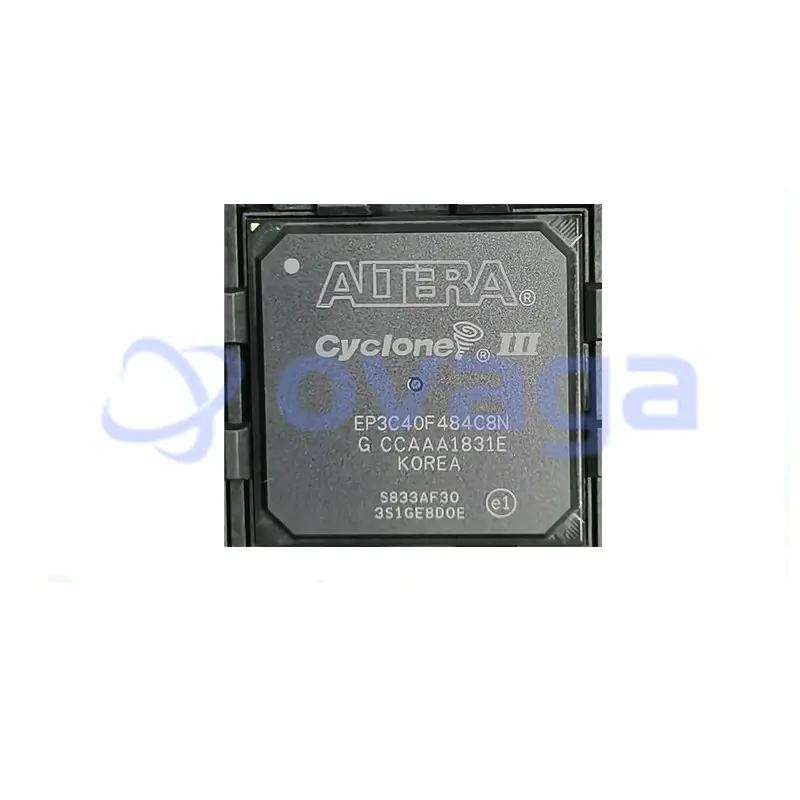
$5000Altera EP3C40F484C8N
With its advanced architecture and high-speed I/O interfaces


Marken: Altera Corporation (Intel)
Herstellerteil #: EP3C40F484C8N
Datenblatt: EP3C40F484C8N Datasheet (PDF)
Paket/Gehäuse: FBGA-484
Produktart: FPGAs (Field Programmable Gate Array)
RoHS-Status:
Lagerzustand: 2.061 Stück, Neues Original
Warranty: 1 Year Ovaga Warranty - Find Out More
0
1
EP3C40F484C8N Allgemeine Beschreibung
The EP3C40F484C8N is a versatile solution for a wide range of applications, including telecommunications, industrial automation, and embedded systems. Its surface mount device termination type simplifies the assembly process, while the FPGA's scalability and flexibility make it a cost-effective choice for prototype development and volume production
Funktionen
- It contains 39,600 logic elements (LEs) and 1,260 embedded memory blocks (MBs).
- It has a maximum of 550 user I/O pins.
- It operates at a maximum frequency of 400 MHz.
- It has various configurable features such as PLLs (Phase-Locked Loops), memory controllers, and transceivers.
Anwendung
- Industrial automation
- Video and image processing
- Network processing
- Medical equipment
- Aerospace and defense systems
- Automotive systems
Spezifikationen
| Parameter | Wert | Parameter | Wert |
|---|---|---|---|
| feature-family-name | Cyclone® III | feature-process-technology | 65nm |
| feature-maximum-number-of-user-i-os | 331 | feature-number-of-registers | |
| feature-device-logic-cells | 39600 | feature-device-system-gates | |
| feature-number-of-multipliers | 126 (18x18) | feature-program-memory-type | SRAM |
| feature-ram-bits-kbit | 1134 | feature-total-number-of-block-ram | 126 |
| feature-ethernet-macs | feature-supported-ip-core | Viterbi Compiler, Low-Speed/Hybrid Serial Decoder|V1 ColdFire|SpeedView Enabled JPEG Encoder (SVE-JPEG-E)|10 Gigabit Ethernet MAC|32/64-bit PCI-X bus Master/Target interface Core, 66/100/133Mhz | |
| feature-supported-ip-core-manufacture | Altera/Freescale/CAST, Inc/MorethanIP/PLDA | feature-maximum-number-of-serdes-channels | |
| feature-device-logic-units | 39600 | feature-device-number-of-dlls-plls | 4 |
| feature-transceiver-blocks | feature-transceiver-speed-gbps | ||
| feature-dedicated-dsp | feature-pci-blocks | ||
| feature-programmability | No | feature-maximum-internal-frequency-mhz | 402 |
| feature-speed-grade | 8 | feature-giga-multiply-accumulates-per-second | |
| feature-differential-i-o-standards-supported | LVPECL|LVDS|HSTL-18|HSTL-15|HSTL-12|SSTL-2|SSTL-18|RSDS | feature-single-ended-i-o-standards-supported | LVTTL|LVCMOS|PCI|PCI-X|SSTL|HSTL |
| feature-external-memory-interface | DDR2 SDRAM|QDRII+SRAM | feature-minimum-operating-supply-voltage-v | 1.15 |
| feature-maximum-operating-supply-voltage-v | 1.25 | feature-packaging | Tray |
| feature-rohs | feature-rad-hard | ||
| feature-pin-count | 484 | feature-supplier-package | FBGA |
| feature-standard-package-name1 | BGA | feature-cecc-qualified | No |
| feature-esd-protection | feature-escc-qualified | ||
| feature-military | No | feature-aec-qualified | No |
| feature-aec-qualified-number | feature-auto-motive | No | |
| feature-p-pap | No | feature-eccn-code | 3A991 |
| feature-svhc | No |
Versand
| Versandart | Versandgebühr | Vorlaufzeit | |
|---|---|---|---|
 |
DHL | $20.00-$40.00 (0.50 KG) | 2-5 Tage |
 |
FedEx | $20.00-$40.00 (0.50 KG) | 2-5 Tage |
 |
UPS | $20.00-$40.00 (0.50 KG) | 2-5 Tage |
 |
TNT | $20.00-$40.00 (0.50 KG) | 2-5 Tage |
 |
EMS | $20.00-$40.00 (0.50 KG) | 2-5 Tage |
 |
REGISTRIERTE LUFTPOST | $20.00-$40.00 (0.50 KG) | 2-5 Tage |
Bearbeitungszeit: Die Versandkosten hängen von der jeweiligen Zone und dem Land ab.
Zahlung
| Zahlungsbedingungen | Handgebühr | |
|---|---|---|
 |
Banküberweisung | Bankgebühr in Höhe von 30,00 USD wird berechnet. |
 |
Paypal | 4,0 % Servicegebühr wird berechnet. |
 |
Kreditkarte | 3,5 % Servicegebühr wird berechnet. |
 |
Western Union | charge US.00 banking fee. |
 |
Geldgramm | Bankgebühr in Höhe von 0,00 USD wird berechnet. |
Garantien
1. Die von Ihnen gekauften elektronischen Bauteile enthalten eine 365-tägige Garantie. Wir garantieren die Produktqualität.
2. Wenn einige der Artikel, die Sie erhalten haben, nicht von perfekter Qualität sind, würden wir verantwortungsvoll Ihre Rückerstattung oder Ersatz arrangieren. Die Artikel müssen jedoch in ihrem Originalzustand verbleiben.
Verpackung
-

Schritt1 :Produkt
-

Schritt2 :Vakuumverpackung
-

Schritt3 :Antistatikbeutel
-

Schritt4 :Individuelle Verpackung
-

Schritt5 :Verpackungskartons
-

Schritt6 :Barcode-Versandetikett


Alle Produkte werden in antistatischen Beuteln verpackt. Versand mit ESD-Antistatikschutz.
Auf dem äußeren ESD-Verpackungsetikett werden die Informationen unseres Unternehmens verwendet: Teilenummer, Marke und Menge.
Wir prüfen alle Waren vor dem Versand, stellen sicher, dass sich alle Produkte in gutem Zustand befinden und dass die Teile neu und original sind und mit dem Datenblatt übereinstimmen.
Nachdem alle Waren darauf überprüft wurden, dass nach dem Verpacken keine Probleme auftreten, werden wir sicher verpacken und per Global Express versenden. Es zeigt eine ausgezeichnete Durchstoß- und Reißfestigkeit sowie eine gute Dichtungsintegrität.


Äquivalente Teile
Für den EP3C40F484C8N Komponente, Sie könnten diese Ersatz- und Alternativteile in Betracht ziehen:
Artikelnummer
Marken
Paket
Beschreibung
Teilpunkte
-
EP3C40F484C8N is a programmable chip developed by Altera. It belongs to the Cyclone III FPGA family and is designed for a broad range of applications. With 40,000 logic elements, 583 I/O pins, and various high-speed interfaces, it offers high performance and flexibility. The C8N package refers to the chip's 484-pin FineLine BGA package. Overall, EP3C40F484C8N is ideal for complex digital systems and offers customization options through its programmable logic.
-
Equivalent
Equivalent products of the EP3C40F484C8N chip include EP3C40F484I8N, EP3C40F484I7N, EP3C40F484I8LN, and EP3C40F484I7LN from the same Cyclone III FPGA family by Altera/Intel. -
Features
EP3C40F484C8N is a Cyclone III FPGA (Field-Programmable Gate Array) with 40,020 logic elements, 1,134 Kbits RAM, and 346 multiplexers. It operates at a maximum clock frequency of 408 MHz and has 249 user I/O pins. This FPGA offers high performance, low power consumption, and is suited for a wide range of applications. -
Pinout
The EP3C40F484C8N is an FPGA with a pin count of 484. Its function is to program and configure digital logic circuits to perform specific tasks. The FPGA can be customized to meet specific requirements and is often used in applications such as telecommunications, image and video processing, and embedded systems. -
Manufacturer
EP3C40F484C8N is manufactured by Altera, which is a company specializing in the production of programmable logic devices and associated software and development tools. Altera, now a part of Intel Corporation, offers a range of FPGA (field-programmable gate array) solutions for various applications in sectors like automotive, telecommunications, industrial automation, and more. -
Application Field
The EP3C40F484C8N is a field-programmable gate array (FPGA) that is commonly used in various applications such as automotive systems, industrial automation, communication systems, and image and video processing. Its high-performance and flexible architecture make it suitable for a wide range of electronic design projects. -
Package
The EP3C40F484C8N chip is offered in a standard plastic package of FBGA (Fine-pitch Ball Grid Array) type. It has 484 contacts and its form, or physical dimensions, are designed for a small footprint, making it suitable for various applications.


Datenblatt PDF
Wir bieten qualitativ hochwertige Produkte, durchdachten Service und eine Kundendienstgarantie
-

Wir haben reichhaltige Produkte, die Ihre unterschiedlichen Bedürfnisse erfüllen können.
-

Die Mindestbestellmenge beginnt bei 1 Stück.
-

Niedrigste internationale Versandgebühr beginnt ab 0,00 USD
-

365 Tage Qualitätsgarantie für alle Produkte


