Bilder dienen nur zur Referenz. Siehe Produktspezifikationen.
Bestellungen über
$5000LCMXO3LF-1300C-5BG256I
This FPGA operates at a voltage of 1.2V and comes in a 256-pin chip-scale package (CABGA) configuration, delivered in a tray format


Marken: Lattice Semiconductor Corporation
Herstellerteil #: LCMXO3LF-1300C-5BG256I
Datenblatt: LCMXO3LF-1300C-5BG256I Datenblatt (PDF)
Paket/Gehäuse: 256-LFBGA
Produktart: FPGAs (Field Programmable Gate Array)
RoHS-Status:
Lagerzustand: 8.745 Stück, Neues Original
Warranty: 1 Year Ovaga Warranty - Find Out More
0
1
LCMXO3LF-1300C-5BG256I Allgemeine Beschreibung
The LCMXO3LF-1300C-5BG256I FPGA, manufactured by Lattice Semiconductor, offers a compelling combination of performance and energy efficiency. With a logic cell count of 1300 and a maximum speed grade of 5, this low-cost, low-power FPGA is capable of handling small to medium-sized designs with ease. Its 256-pin BGA package ensures a compact form factor, making it a great fit for space-constrained applications, while its low power consumption makes it ideal for mobile devices, IoT applications, and other battery-powered devices. Additionally, the LCMXO3LF-1300C-5BG256I boasts embedded block RAM, DSP blocks, and flexible I/O options, allowing for versatile and efficient design implementations across a wide range of applications
Funktionen
- Non-volatile, Infinitely Reconfigurable
- Instant-on – powers up in microseconds
- Single chip, no external configuration memory
- required
- Excellent design security, no bit stream to
- intercept
- Reconfigure SRAM based logic in milliseconds
- SRAM and non-volatile memory programmable
- through JTAG port
- Supports background programming of
- non-volatile memory
- Sleep Mode
- Allows up to 100x static current reduction
- TransFR™ Reconfiguration (TFR)
- In-field logic update while system operates
- High I/O to Logic Density
- 256 to 2280 LUT4s
- 73 to 271 I/Os with extensive package options
- Density migration supported
- Lead free/RoHS compliant packaging
- Embedded and Distributed Memory
- Up to 27.6 Kbits sysMEM™ Embedded Block
- Up to 7.5 Kbits distributed RAM
- Dedicated FIFO control logic
- Flexible I/O Buffer
- Programmable sysIO™ buffer supports wide
- range of interfaces:
- − LVCMOS 3.3/2.5/1.8/1.5/1.2
- − LVTTL
- − LVDS, Bus-LVDS, LVPECL, RSDS
- sysCLOCK™ PLLs
- Up to two analog PLLs per device
- Clock multiply, divide, and phase shifting
- System Level Support
- IEEE Standard 1149.1 Boundary Scan
- Onboard oscillator
- Devices operate with 3.3V, 2.5V, 1.8V or 1.2V
- power supply
- IEEE 1532 compliant in-system programming
Spezifikationen
| Parameter | Wert | Parameter | Wert |
|---|---|---|---|
| Series | MachXO3 | Package | Tray |
| Product Status | Active | Programmabe | Not Verified |
| Number of LABs/CLBs | 160 | Number of Logic Elements/Cells | 1280 |
| Total RAM Bits | 65536 | Number of I/O | 206 |
| Voltage - Supply | 2.375V ~ 3.465V | Mounting Type | Surface Mount |
| Operating Temperature | -40°C ~ 100°C (TJ) | Package / Case | 256-LFBGA |
| Supplier Device Package | 256-CABGA (14x14) |
Versand
| Versandart | Versandgebühr | Vorlaufzeit | |
|---|---|---|---|
 |
DHL | $20.00-$40.00 (0.50 KG) | 2-5 Tage |
 |
FedEx | $20.00-$40.00 (0.50 KG) | 2-5 Tage |
 |
UPS | $20.00-$40.00 (0.50 KG) | 2-5 Tage |
 |
TNT | $20.00-$40.00 (0.50 KG) | 2-5 Tage |
 |
EMS | $20.00-$40.00 (0.50 KG) | 2-5 Tage |
 |
REGISTRIERTE LUFTPOST | $20.00-$40.00 (0.50 KG) | 2-5 Tage |
Bearbeitungszeit: Die Versandkosten hängen von der jeweiligen Zone und dem Land ab.
Zahlung
| Zahlungsbedingungen | Handgebühr | |
|---|---|---|
 |
Banküberweisung | Bankgebühr in Höhe von 30,00 USD wird berechnet. |
 |
Paypal | 4,0 % Servicegebühr wird berechnet. |
 |
Kreditkarte | 3,5 % Servicegebühr wird berechnet. |
 |
Western Union | charge US.00 banking fee. |
 |
Geldgramm | Bankgebühr in Höhe von 0,00 USD wird berechnet. |
Garantien
1. Die von Ihnen gekauften elektronischen Bauteile enthalten eine 365-tägige Garantie. Wir garantieren die Produktqualität.
2. Wenn einige der Artikel, die Sie erhalten haben, nicht von perfekter Qualität sind, würden wir verantwortungsvoll Ihre Rückerstattung oder Ersatz arrangieren. Die Artikel müssen jedoch in ihrem Originalzustand verbleiben.
Verpackung
-

Schritt1 :Produkt
-

Schritt2 :Vakuumverpackung
-

Schritt3 :Antistatikbeutel
-

Schritt4 :Individuelle Verpackung
-

Schritt5 :Verpackungskartons
-

Schritt6 :Barcode-Versandetikett


Alle Produkte werden in antistatischen Beuteln verpackt. Versand mit ESD-Antistatikschutz.
Auf dem äußeren ESD-Verpackungsetikett werden die Informationen unseres Unternehmens verwendet: Teilenummer, Marke und Menge.
Wir prüfen alle Waren vor dem Versand, stellen sicher, dass sich alle Produkte in gutem Zustand befinden und dass die Teile neu und original sind und mit dem Datenblatt übereinstimmen.
Nachdem alle Waren darauf überprüft wurden, dass nach dem Verpacken keine Probleme auftreten, werden wir sicher verpacken und per Global Express versenden. Es zeigt eine ausgezeichnete Durchstoß- und Reißfestigkeit sowie eine gute Dichtungsintegrität.


Teilpunkte
-
The LCMXO3LF-1300C-5BG256I chip is a low-power, small-footprint FPGA (field-programmable gate array) from Lattice Semiconductor. It features 1300 LUTs, 317 Kbits of embedded memory, and 36 I/Os. This chip is ideal for applications requiring low power consumption and space constraints.
-
Equivalent
The equivalent products of the LCMXO3LF-1300C-5BG256I chip are the LCMXO3 series from Lattice Semiconductor, including the LCMXO3LF-1300C-6BG256I and the LCMXO3LF-1300C-6BG324I. These chips offer similar features and functionality, providing alternative options for design and integration. -
Features
LCMXO3LF-1300C-5BG256I features 1300 LUTs, 640 macrocells, 6 kilobits of RAM, 32 I/Os, and is housed in a 256-ball grid array package. It has low power consumption, small form factor, and is ideal for low power applications in industrial, consumer, and automotive markets. -
Pinout
The LCMXO3LF-1300C-5BG256I is a low-power FPGA with 256 pins. It is designed for use in low-power applications and features 1300 LUTs. It also includes 4 Multiplier/Accumulators and 32 I/O pins. -
Manufacturer
LCMXO3LF-1300C-5BG256I is manufactured by Lattice Semiconductor Corporation, a company specializing in low-power, small form-factor programmable logic devices. Lattice Semiconductor Corporation is a leading provider of smart connectivity solutions, offering customizable solutions for a wide range of applications in consumer, automotive, industrial, and communications markets. -
Application Field
The LCMXO3LF-1300C-5BG256I can be used in a variety of application areas such as battery management systems, sensor interfaces, portable medical devices, and industrial automation. Its low power consumption, small form factor, and high integration make it ideal for applications requiring low power consumption and high performance in a compact package. -
Package
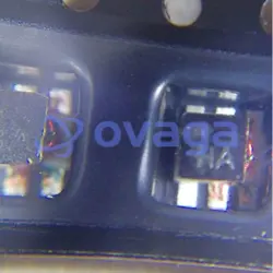
The LCMXO3LF-1300C-5BG256I chip is in a 256-ball Fine-pitch Ball Grid Array (FPBGA) package. It is a Field-Programmable Gate Array (FPGA) in a form of a chip. The size of the chip is 13mm x 13mm.


Wir bieten qualitativ hochwertige Produkte, durchdachten Service und eine Kundendienstgarantie
-

Wir haben reichhaltige Produkte, die Ihre unterschiedlichen Bedürfnisse erfüllen können.
-

Die Mindestbestellmenge beginnt bei 1 Stück.
-

Niedrigste internationale Versandgebühr beginnt ab 0,00 USD
-

365 Tage Qualitätsgarantie für alle Produkte