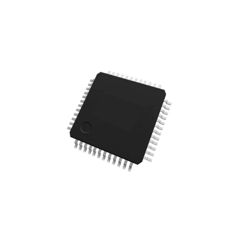
Bilder dienen nur zur Referenz. Siehe Produktspezifikationen.
Bestellungen über
$5000
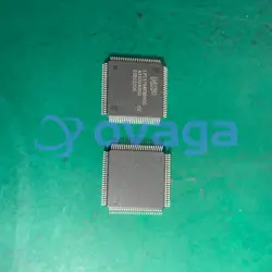
LPC1754FBD80,518

80-Pin LQFP Package


Marken: NXP SEMICONDUCTORS
Herstellerteil #: LPC1754FBD80,518
Datenblatt: LPC1754FBD80,518 Datenblatt (PDF)
Paket/Gehäuse: LQFP-80
RoHS-Status:
Lagerzustand: 5.792 Stück, Neues Original
Produktart: Microcontrollers
Warranty: 1 Year Ovaga Warranty - Find Out More
0
1
*Alle Preise sind in USD
| Menge | Einzelpreis | Ext. Preis |
|---|---|---|
| 1 | $9,232 | $9,232 |
| 10 | $8,098 | $80,980 |
| 30 | $7,408 | $222,240 |
| 100 | $6,828 | $682,800 |
Auf Lager: 5.792 Stck
LPC1754FBD80,518 Allgemeine Beschreibung
Embedded developers will find the LPC1754FBD80,518 microcontroller to be a versatile platform for a multitude of communication interfaces, including UART, SPI, I2C, and CAN, as well as USB connectivity. This broad spectrum of communication options enables seamless integration with a variety of peripheral devices and networks. Additionally, the microcontroller's abundant timers, PWM channels, analog peripherals, and GPIO pins afford ample flexibility for interfacing with sensors, actuators, and other external hardware components
Funktionen
- ARM Cortex-M3 processor, running at frequencies of up to 100 MHz
- (LPC1758/56/57/54/52/51) or of up to 120 MHz (LPC1759). A Memory Protection Unit
- (MPU) supporting eight regions is included.
- ARM Cortex-M3 built-in Nested Vectored Interrupt Controller (NVIC).
- Up to 512 kB on-chip flash programming memory. Enhanced flash memory accelerator enables high-speed 120 MHz operation with zero wait states.
- In-System Programming (ISP) and In-Application Programming (IAP) via on-chip bootloader software.
- On-chip SRAM includes:
- ♦ Up to 32 kB of SRAM on the CPU with local code/data bus for high-performance CPU access.
- ♦ Two/one 16 kB SRAM blocks with separate access paths for higher throughput.
- These SRAM blocks may be used for Ethernet (LPC1758 only), USB, and DMA memory, as well as for general purpose CPU instruction and data storage.
- Eight channel General Purpose DMA controller (GPDMA) on the AHB multilayer matrix that can be used with the SSP, I2S-bus, UART, the Analog-to-Digital and Digital-to-Analog converter peripherals, timer match signals, and for memory-to-memory transfers.
- Multilayer AHB matrix interconnect provides a separate bus for each AHB master. AHB masters include the CPU, General Purpose DMA controller, Ethernet MAC (LPC1758 only), and the USB interface. This interconnect provides communication with no arbitration delays.
- Split APB bus allows high throughput with few stalls between the CPU and DMA.
- Serial interfaces:
- ♦ On the LPC1758 only, Ethernet MAC with RMII interface and dedicated DMA controller.
- ♦ USB 2.0 full-speed device/Host/OTG controller with dedicated DMA controller and on-chip PHY for device, Host, and OTG functions. The LPC1752/51 include a USB device controller only.
- ♦ Four UARTs with fractional baud rate generation, internal FIFO, and DMA support. One UART has modem control I/O and RS-485/EIA-485 support, and one UART has IrDA support.
- ♦ CAN 2.0B controller with two (LPC1759/58/56) or one (LPC1754/52/51) channels.
- ♦ SPI controller with synchronous, serial, full duplex communication and programmable data length.
- ♦ Two SSP controllers with FIFO and multi-protocol capabilities. The SSP interfaces can be used with the GPDMA controller.
- ♦ Two I2C-bus interfaces supporting fast mode with a data rate of 400 kbit/s with multiple address recognition and monitor mode.
- ♦ On the LPC1759/58/56 only, I2S (Inter-IC Sound) interface for digital audio input or output, with fractional rate control. The I2S-bus interface can be used with the GPDMA. The I2S-bus interface supports 3-wire and 4-wire data transmit and receive as well as master clock input/output.
- Other peripherals:
- ♦ 52 General Purpose I/O (GPIO) pins with configurable pull-up/down resistors. All GPIOs support a new, configurable open-drain operating mode. The GPIO block is accessed through the AHB multilayer bus for fast access and located in memory such that it supports Cortex-M3 bit banding and use by the General Purpose DMA Controller.
- ♦ 12-bit Analog-to-Digital Converter (ADC) with input multiplexing among six pins, conversion rates up to 200 kHz, and multiple result registers. The 12-bit ADC can be used with the GPDMA controller.
- ♦ On the LPC1759/58/56/54 only, 10-bit Digital-to-Analog Converter (DAC) with dedicated conversion timer and DMA support.
- Four general purpose timers/counters, with a total of three capture inputs and ten compare outputs. Each timer block has an external count input. Specific timer events can be selected to generate DMA requests.
- ♦ One motor control PWM with support for three-phase motor control.
- ♦ Quadrature encoder interface that can monitor one external quadrature encoder.
- ♦ One standard PWM/timer block with external count input.
- ♦ Real-Time Clock (RTC) with a separate power domain and dedicated RTC oscillator. The RTC block includes 20 bytes of battery-powered backup registers.
- ♦ WatchDog Timer (WDT). The WDT can be clocked from the internal RC oscillator, the RTC oscillator, or the APB clock.
- ♦ ARM Cortex-M3 system tick timer, including an external clock input option.
- ♦ Repetitive Interrupt Timer (RIT) provides programmable and repeating timed interrupts.
- ♦ Each peripheral has its own clock divider for further power savings.
Spezifikationen
| Parameter | Wert | Parameter | Wert |
|---|---|---|---|
| Source Content uid | LPC1754FBD80,518 | Rohs Code | Yes |
| Part Life Cycle Code | Active | Ihs Manufacturer | NXP SEMICONDUCTORS |
| Part Package Code | QFP | Package Description | LFQFP, QFP80,.55SQ,20 |
| Pin Count | 80 | Manufacturer Package Code | SOT315-1 |
| Reach Compliance Code | compliant | HTS Code | 8542.31.00.01 |
| Factory Lead Time | 52 Weeks | Samacsys Manufacturer | NXP |
| Has ADC | YES | Address Bus Width | |
| Bit Size | 32 | Clock Frequency-Max | 25 MHz |
| DAC Channels | NO | DMA Channels | YES |
| External Data Bus Width | JESD-30 Code | S-PQFP-G80 | |
| JESD-609 Code | e3 | Length | 12 mm |
| Moisture Sensitivity Level | 2 | Number of I/O Lines | 52 |
| Number of Terminals | 80 | Operating Temperature-Max | 85 °C |
| Operating Temperature-Min | -40 °C | PWM Channels | YES |
| Package Body Material | PLASTIC/EPOXY | Package Code | LFQFP |
| Package Equivalence Code | QFP80,.55SQ,20 | Package Shape | SQUARE |
| Package Style | FLATPACK, LOW PROFILE, FINE PITCH | Peak Reflow Temperature (Cel) | 260 |
| Power Supplies | 3.3 V | Qualification Status | Not Qualified |
| RAM (bytes) | 32768 | ROM (words) | 131072 |
| ROM Programmability | FLASH | Seated Height-Max | 1.6 mm |
| Speed | 100 MHz | Supply Current-Max | 100 mA |
| Supply Voltage-Max | 3.6 V | Supply Voltage-Min | 2.4 V |
| Supply Voltage-Nom | 3.3 V | Surface Mount | YES |
| Technology | CMOS | Temperature Grade | INDUSTRIAL |
| Terminal Finish | TIN | Terminal Form | GULL WING |
| Terminal Pitch | 0.5 mm | Terminal Position | QUAD |
| Time@Peak Reflow Temperature-Max (s) | 30 | Width | 12 mm |
| uPs/uCs/Peripheral ICs Type | MICROCONTROLLER, RISC | Series | LPC17xx |
| Product Status | Active | Programmabe | Not Verified |
| Core Processor | ARM® Cortex®-M3 | Core Size | 32-Bit Single-Core |
| Connectivity | CANbus, I2C, IrDA, Microwire, SPI, SSI, SSP, UART/USART, USB OTG | Peripherals | Brown-out Detect/Reset, DMA, Motor Control PWM, POR, PWM, WDT |
| Number of I/O | 52 | Program Memory Size | 128KB (128K x 8) |
| Program Memory Type | FLASH | RAM Size | 32K x 8 |
| Voltage - Supply (Vcc/Vdd) | 2.4V ~ 3.6V | Data Converters | A/D 6x12b; D/A 1x10b |
| Oscillator Type | Internal | Operating Temperature | -40°C ~ 85°C (TA) |
| Mounting Type | Surface Mount | Package / Case | 80-LQFP |
| Supplier Device Package | 80-LQFP (12x12) |
Versand
| Versandart | Versandgebühr | Vorlaufzeit | |
|---|---|---|---|
 |
DHL | $20.00-$40.00 (0.50 KG) | 2-5 Tage |
 |
FedEx | $20.00-$40.00 (0.50 KG) | 2-5 Tage |
 |
UPS | $20.00-$40.00 (0.50 KG) | 2-5 Tage |
 |
TNT | $20.00-$40.00 (0.50 KG) | 2-5 Tage |
 |
EMS | $20.00-$40.00 (0.50 KG) | 2-5 Tage |
 |
REGISTRIERTE LUFTPOST | $20.00-$40.00 (0.50 KG) | 2-5 Tage |
Bearbeitungszeit: Die Versandkosten hängen von der jeweiligen Zone und dem Land ab.
Zahlung
| Zahlungsbedingungen | Handgebühr | |
|---|---|---|
 |
Banküberweisung | Bankgebühr in Höhe von 30,00 USD wird berechnet. |
 |
Paypal | 4,0 % Servicegebühr wird berechnet. |
 |
Kreditkarte | 3,5 % Servicegebühr wird berechnet. |
 |
Western Union | charge US.00 banking fee. |
 |
Geldgramm | Bankgebühr in Höhe von 0,00 USD wird berechnet. |
Garantien
1. Die von Ihnen gekauften elektronischen Bauteile enthalten eine 365-tägige Garantie. Wir garantieren die Produktqualität.
2. Wenn einige der Artikel, die Sie erhalten haben, nicht von perfekter Qualität sind, würden wir verantwortungsvoll Ihre Rückerstattung oder Ersatz arrangieren. Die Artikel müssen jedoch in ihrem Originalzustand verbleiben.
Verpackung
-

Schritt1 :Produkt
-

Schritt2 :Vakuumverpackung
-

Schritt3 :Antistatikbeutel
-

Schritt4 :Individuelle Verpackung
-

Schritt5 :Verpackungskartons
-

Schritt6 :Barcode-Versandetikett


Alle Produkte werden in antistatischen Beuteln verpackt. Versand mit ESD-Antistatikschutz.
Auf dem äußeren ESD-Verpackungsetikett werden die Informationen unseres Unternehmens verwendet: Teilenummer, Marke und Menge.
Wir prüfen alle Waren vor dem Versand, stellen sicher, dass sich alle Produkte in gutem Zustand befinden und dass die Teile neu und original sind und mit dem Datenblatt übereinstimmen.
Nachdem alle Waren darauf überprüft wurden, dass nach dem Verpacken keine Probleme auftreten, werden wir sicher verpacken und per Global Express versenden. Es zeigt eine ausgezeichnete Durchstoß- und Reißfestigkeit sowie eine gute Dichtungsintegrität.


Wir bieten qualitativ hochwertige Produkte, durchdachten Service und eine Kundendienstgarantie
-

Wir haben reichhaltige Produkte, die Ihre unterschiedlichen Bedürfnisse erfüllen können.
-

Die Mindestbestellmenge beginnt bei 1 Stück.
-

Niedrigste internationale Versandgebühr beginnt ab 0,00 USD
-

365 Tage Qualitätsgarantie für alle Produkte