

Bilder dienen nur zur Referenz. Siehe Produktspezifikationen.
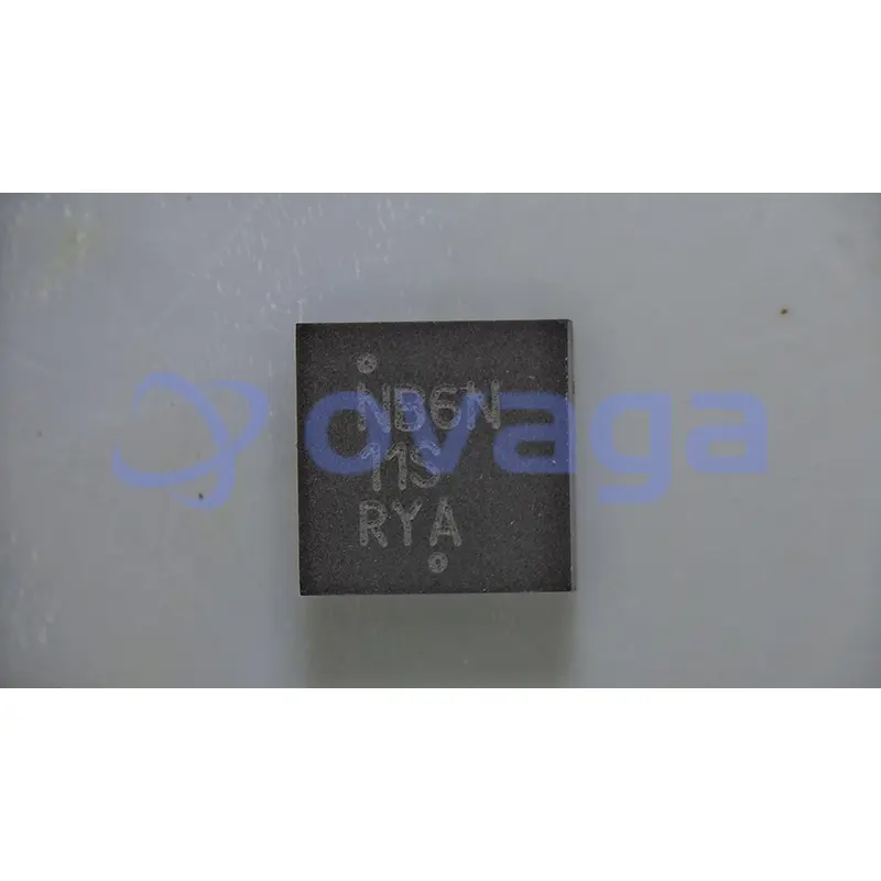
ON NB6N11SMNG
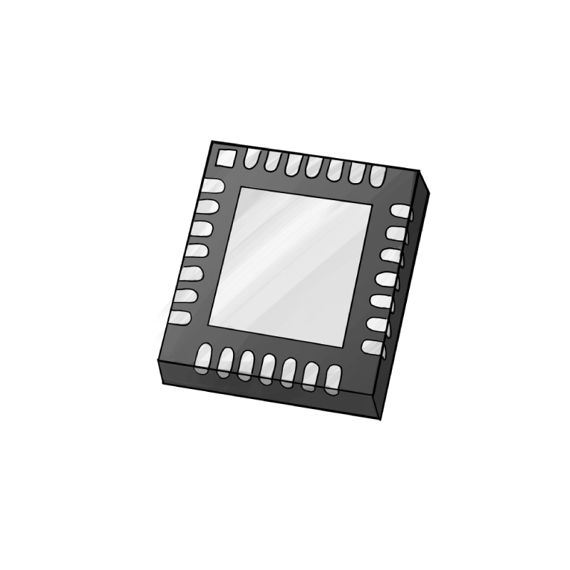
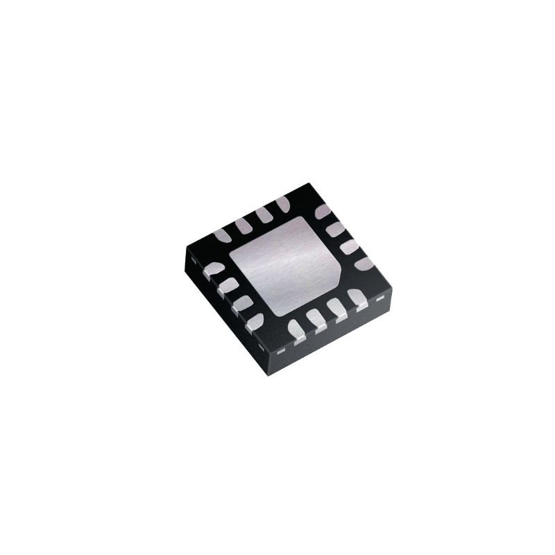
Clock Fanout Buffer (Distribution), Translator IC 1:2 2 GHz 16-VFQFN Exposed Pad


Marken: ON Semiconductor, LLC
Herstellerteil #: NB6N11SMNG
Datenblatt: NB6N11SMNG Datasheet (PDF)
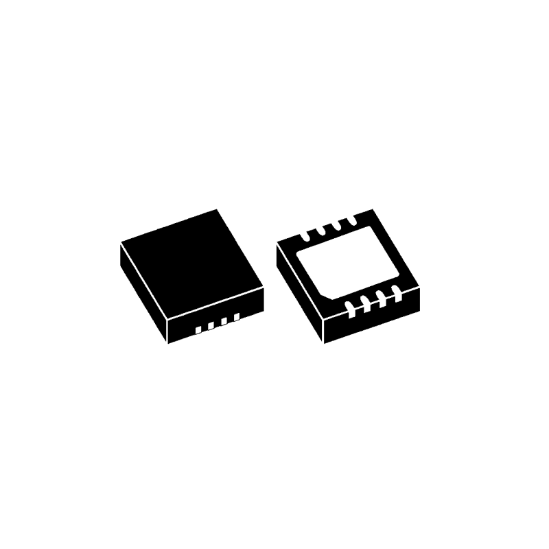
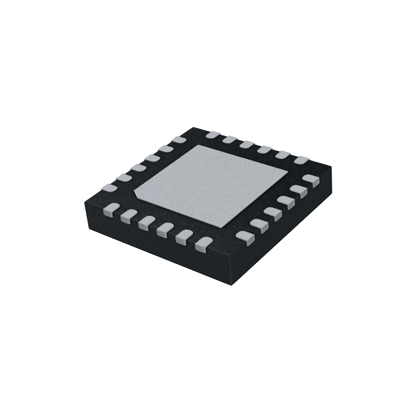
Paket/Gehäuse: QFN-16 EP
Produktart: Uhren- & Timer-ICs
RoHS-Status:
Lagerzustand: 3641 Stück, Neues Original
Warranty: 1 Year Ovaga Warranty - Find Out More
0
1
BOMNB6N11SMNG Allgemeine Beschreibung
The NB6N11S is a differential 1:2 Clock or Data Receiver and will accept AnyLevelTM input signals: LVPECL, CML, LVCMOS, LVTTL, or LVDS. These signals will be translated to LVDS and two identical copies of Clock or Data will be distributed, operating up to 2.0 GHz or 2.5 Gb/s, respectively. As such, the NB6N11S is ideal for SONET, GigE, Fiber Channel, Backplane and other Clock or Data distribution applications. The NB6N11S has a wide input common mode range from GND + 50mV to VCC - 50 mV. Combined with the 50-ohm internal termination resistors at the inputs, the NB6N11S is ideal for translating a variety of differential or single-ended Clock or Data signals to 350 mV typical LVDS output levels. The NB6N11S is functionally equivalent to the EP11, LVEP11, SG11 or 7L11M devices and is offered in a small 3mm X 3mm 16-QFN package.
Funktionen
- Maximum Input Clock Frequency > 2.0 GHz
- Maximum Input Data Rate > 2.5 Gb/s
- 1 ps Maximum of RMS Clock Jitter
- Typically 10 ps of Data Dependent Jitter
- 380 ps Typical Propagation Delay
- 120 ps Typical Rise and Fall Times
- These devices are available in Pb-free package(s). Specifications herein
Anwendung
- High Performance LVDS Clock and Data Distribution for ATE and Networking
Spezifikationen
| Parameter | Wert | Parameter | Wert |
|---|---|---|---|
| Source Content uid | NB6N11SMNG | Pbfree Code | Yes |
| Part Life Cycle Code | Active | Ihs Manufacturer | ONSEMI |
| Part Package Code | QFN16, 3x3, 0.5P | Package Description | QFN-16 |
| Pin Count | 16 | Manufacturer Package Code | 485G-01 |
| Reach Compliance Code | compliant | HTS Code | 8542.39.00.01 |
| Factory Lead Time | 39 Weeks | Samacsys Manufacturer | onsemi |
| Family | 6N | Input Conditioning | DIFFERENTIAL |
| JESD-30 Code | S-XQCC-N16 | Logic IC Type | LOW SKEW CLOCK DRIVER |
| Moisture Sensitivity Level | 1 | Number of Functions | 1 |
| Number of Inverted Outputs | Number of Terminals | 16 | |
| Number of True Outputs | 4 | Package Body Material | UNSPECIFIED |
| Package Code | HVQCCN | Package Equivalence Code | LCC16,.12SQ,20 |
| Package Shape | SQUARE | Package Style | CHIP CARRIER, HEAT SINK/SLUG, VERY THIN PROFILE |
| Peak Reflow Temperature (Cel) | 260 | Surface Mount | YES |
| Temperature Grade | INDUSTRIAL | Terminal Finish | NICKEL GOLD PALLADIUM |
| Terminal Form | NO LEAD | Terminal Position | QUAD |
| Time@Peak Reflow Temperature-Max (s) | 30 | feature-maximum-operating-supply-voltage-v | 3.6 |
| feature-minimum-operating-supply-voltage-v | 3 | feature-packaging | Rail |
| feature-rad-hard | feature-pin-count | 16 | |
| feature-supplier-package | QFN EP | feature-standard-package-name1 | QFN |
| feature-cecc-qualified | No | feature-esd-protection | Yes |
| feature-military | No | feature-aec-qualified | No |
| feature-aec-qualified-number | feature-auto-motive | No | |
| feature-p-pap | No | feature-eccn-code | EAR99 |
| feature-svhc | No |
Versand
| Versandart | Versandgebühr | Vorlaufzeit | |
|---|---|---|---|
 |
DHL | $20.00-$40.00 (0.50 KG) | 2-5 Tage |
 |
FedEx | $20.00-$40.00 (0.50 KG) | 2-5 Tage |
 |
UPS | $20.00-$40.00 (0.50 KG) | 2-5 Tage |
 |
TNT | $20.00-$40.00 (0.50 KG) | 2-5 Tage |
 |
EMS | $20.00-$40.00 (0.50 KG) | 2-5 Tage |
 |
REGISTRIERTE LUFTPOST | $20.00-$40.00 (0.50 KG) | 2-5 Tage |
Bearbeitungszeit: Die Versandkosten hängen von der jeweiligen Zone und dem Land ab.
Zahlung
| Zahlungsbedingungen | Handgebühr | |
|---|---|---|
 |
Banküberweisung | Bankgebühr in Höhe von 30,00 USD wird berechnet. |
 |
Paypal | 4,0 % Servicegebühr wird berechnet. |
 |
Kreditkarte | 3,5 % Servicegebühr wird berechnet. |
 |
Western Union | charge US.00 banking fee. |
 |
Geldgramm | Bankgebühr in Höhe von 0,00 USD wird berechnet. |
Garantien
1. Die von Ihnen gekauften elektronischen Bauteile enthalten eine 365-tägige Garantie. Wir garantieren die Produktqualität.
2. Wenn einige der Artikel, die Sie erhalten haben, nicht von perfekter Qualität sind, würden wir verantwortungsvoll Ihre Rückerstattung oder Ersatz arrangieren. Die Artikel müssen jedoch in ihrem Originalzustand verbleiben.
Verpackung
-

Schritt1 :Produkt
-

Schritt2 :Vakuumverpackung
-

Schritt3 :Antistatikbeutel
-

Schritt4 :Individuelle Verpackung
-

Schritt5 :Verpackungskartons
-

Schritt6 :Barcode-Versandetikett


Alle Produkte werden in antistatischen Beuteln verpackt. Versand mit ESD-Antistatikschutz.
Auf dem äußeren ESD-Verpackungsetikett werden die Informationen unseres Unternehmens verwendet: Teilenummer, Marke und Menge.
Wir prüfen alle Waren vor dem Versand, stellen sicher, dass sich alle Produkte in gutem Zustand befinden und dass die Teile neu und original sind und mit dem Datenblatt übereinstimmen.
Nachdem alle Waren darauf überprüft wurden, dass nach dem Verpacken keine Probleme auftreten, werden wir sicher verpacken und per Global Express versenden. Es zeigt eine ausgezeichnete Durchstoß- und Reißfestigkeit sowie eine gute Dichtungsintegrität.


Teilpunkte
-
The NB6N11SMNG is a high-performance clock driver chip designed specifically for applications requiring low phase noise and low voltage swing. It provides 6 output channels with programmable outputs enabling fine control over electrical characteristics. It operates at low power consumption and is suitable for various high-speed data communication systems.
-
Equivalent
Some equivalent products of the NB6N11SMNG chip include the NB6L11SMNG, NB6N14SMNG, and NB6N239SMNG. -
Features
The features of NB6N11SMNG include low power consumption, high speed performance, small size, and low output skew. It is a versatile clock and data buffer IC designed for use in networking, telecommunications, and other high-speed communication applications. -
Pinout
The NB6N11SMNG is a flat clock buffer with 1:2 Fanout. It has a pin count of 8 and functions as a high-performance clock distribution solution for demanding applications. -
Manufacturer
ON Semiconductor is the manufacturer of the NB6N11SMNG. It is a semiconductor manufacturing company that specializes in producing a wide range of electronic components, including integrated circuits and discrete devices. -
Application Field
The NB6N11SMNG is commonly used in various applications, including data communication, networking, and clock distribution systems. It can be found in routers, switches, data centers, and other electronic devices where precise and reliable clock synchronization is required. It helps ensure accurate data transmission and timing synchronization, making it an essential component in modern communication systems. -
Package
The NB6N11SMNG chip is available in a surface mount package with 8 leads. Its form factor is in a small outline integrated circuit (SOIC) package. The dimensions of the package are typically around 3.91mm x 4.90mm.

Datenblatt PDF
Wir bieten qualitativ hochwertige Produkte, durchdachten Service und eine Kundendienstgarantie
-

Wir haben reichhaltige Produkte, die Ihre unterschiedlichen Bedürfnisse erfüllen können.
-

Die Mindestbestellmenge beginnt bei 1 Stück.
-

Niedrigste internationale Versandgebühr beginnt ab 0,00 USD
-

365 Tage Qualitätsgarantie für alle Produkte


Excellent selection of components and competitive pricing. Thanks, Ovaga!