

Bilder dienen nur zur Referenz. Siehe Produktspezifikationen.
ON NC7WV07P6X
Buffer, Non-Inverting 2 Element 1 Bit per Element Open Drain Output SC-88 (SC-70-6)


Marken: ON Semiconductor, LLC
Herstellerteil #: NC7WV07P6X
Datenblatt: NC7WV07P6X Datasheet (PDF)
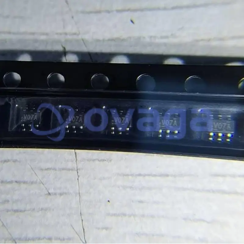
Paket/Gehäuse: SC-70-6
Produktart: Logik-ICs
RoHS-Status:
Lagerzustand: 3547 Stück, Neues Original
Warranty: 1 Year Ovaga Warranty - Find Out More
0
1
BOMNC7WV07P6X Allgemeine Beschreibung
The NC7WV07 is a dual buffer with open drain output from ON Semiconductor's Ultra Low Power-A series of TinyLogic®. ULP-A is ideal for applications that require extreme high speed, high drive and low power. This product is designed for a wide low voltage operating range (0.9V to 3.6V VCC) and applications that require more drive and speed than the TinyLogic ULP series, but still offer best in class low power operation.
The NC7WV07 is uniquely designed for optimized power and speed, and is fabricated with an advanced CMOS technology to achieve high-speed operation while maintaining low CMOS power dissipation.
Funktionen
- 0.9V to 3.6V VCC supply operation
- 3.6V overvoltage tolerant I/O's at VCC from 0.9V to 3.6V
- Extremely High Speed tPD1.0 ns typ for 2.7V to 3.6V VCC1.2 ns typ for 2.3V to 2.7V VCC2.0 ns typ for 1.65V to 1.95V VCC3.2 ns typ for 1.4V to 1.6V VCC6.0 ns typ for 1.1V to 1.3V VCC13.0 ns typ for 0.9V VCC
- Power-Off high impedance inputs and outputs
- High Static Drive (IOH/IOL)±24 mA @ 3.00V VCC±18 mA @ 2.30V VCC±6 mA @ 1.65V VCC±4 mA @ 1.4V VCC±2 mA @ 1.1V VCC±0.1 mA @ 0.9V VCC
- Uses patented Quiet Series™ noise/EMI reduction circuitry
- Ultra small MicroPak™ leadfree package
- Ultra low dynamic power
Anwendung
- This product is general usage and suitable for many different applications.
Spezifikationen
| Parameter | Wert | Parameter | Wert |
|---|---|---|---|
| Source Content uid | NC7WV07P6X | Pbfree Code | Yes |
| Part Life Cycle Code | Active | Ihs Manufacturer | ONSEMI |
| Package Description | SC-88, 6 PIN | Manufacturer Package Code | 419AD |
| Reach Compliance Code | compliant | HTS Code | 8542.39.00.01 |
| Factory Lead Time | 75 Weeks, 5 Days | Samacsys Manufacturer | onsemi |
| Family | AUP/ULP/V | JESD-30 Code | R-PDSO-G6 |
| Logic IC Type | BUFFER | Moisture Sensitivity Level | 1 |
| Number of Functions | 2 | Number of Inputs | 1 |
| Number of Terminals | 6 | Output Characteristics | OPEN-DRAIN |
| Package Body Material | PLASTIC/EPOXY | Package Code | TSSOP |
| Package Equivalence Code | TSSOP6,.08 | Package Shape | RECTANGULAR |
| Package Style | SMALL OUTLINE, THIN PROFILE, SHRINK PITCH | Packing Method | TR |
| Peak Reflow Temperature (Cel) | 260 | Schmitt Trigger | NO |
| Surface Mount | YES | Technology | CMOS |
| Terminal Finish | NICKEL PALLADIUM GOLD | Terminal Form | GULL WING |
| Terminal Position | DUAL | Time@Peak Reflow Temperature-Max (s) | 30 |
| feature-logic-family | WV | feature-logic-function | Buffer/Driver |
| feature-number-of-elements-per-chip | 2 | feature-process-technology | CMOS |
| feature-maximum-low-level-output-current-ma | 24 | feature-output-type | Open Drain |
| feature-minimum-operating-supply-voltage-v | 0.9 | feature-maximum-operating-supply-voltage-v | 3.6 |
| feature-maximum-high-level-output-current-ma | -24 | feature-packaging | Tape and Reel |
| feature-rad-hard | feature-pin-count | 6 | |
| feature-supplier-package | SC-70 | feature-standard-package-name1 | SOT |
| feature-cecc-qualified | No | feature-esd-protection | |
| feature-military | No | feature-aec-qualified | No |
| feature-aec-qualified-number | feature-auto-motive | No | |
| feature-p-pap | No | feature-eccn-code | EAR99 |
| feature-svhc | No |
Versand
| Versandart | Versandgebühr | Vorlaufzeit | |
|---|---|---|---|
 |
DHL | $20.00-$40.00 (0.50 KG) | 2-5 Tage |
 |
FedEx | $20.00-$40.00 (0.50 KG) | 2-5 Tage |
 |
UPS | $20.00-$40.00 (0.50 KG) | 2-5 Tage |
 |
TNT | $20.00-$40.00 (0.50 KG) | 2-5 Tage |
 |
EMS | $20.00-$40.00 (0.50 KG) | 2-5 Tage |
 |
REGISTRIERTE LUFTPOST | $20.00-$40.00 (0.50 KG) | 2-5 Tage |
Bearbeitungszeit: Die Versandkosten hängen von der jeweiligen Zone und dem Land ab.
Zahlung
| Zahlungsbedingungen | Handgebühr | |
|---|---|---|
 |
Banküberweisung | Bankgebühr in Höhe von 30,00 USD wird berechnet. |
 |
Paypal | 4,0 % Servicegebühr wird berechnet. |
 |
Kreditkarte | 3,5 % Servicegebühr wird berechnet. |
 |
Western Union | charge US.00 banking fee. |
 |
Geldgramm | Bankgebühr in Höhe von 0,00 USD wird berechnet. |
Garantien
1. Die von Ihnen gekauften elektronischen Bauteile enthalten eine 365-tägige Garantie. Wir garantieren die Produktqualität.
2. Wenn einige der Artikel, die Sie erhalten haben, nicht von perfekter Qualität sind, würden wir verantwortungsvoll Ihre Rückerstattung oder Ersatz arrangieren. Die Artikel müssen jedoch in ihrem Originalzustand verbleiben.
Verpackung
-

Schritt1 :Produkt
-

Schritt2 :Vakuumverpackung
-

Schritt3 :Antistatikbeutel
-

Schritt4 :Individuelle Verpackung
-

Schritt5 :Verpackungskartons
-

Schritt6 :Barcode-Versandetikett


Alle Produkte werden in antistatischen Beuteln verpackt. Versand mit ESD-Antistatikschutz.
Auf dem äußeren ESD-Verpackungsetikett werden die Informationen unseres Unternehmens verwendet: Teilenummer, Marke und Menge.
Wir prüfen alle Waren vor dem Versand, stellen sicher, dass sich alle Produkte in gutem Zustand befinden und dass die Teile neu und original sind und mit dem Datenblatt übereinstimmen.
Nachdem alle Waren darauf überprüft wurden, dass nach dem Verpacken keine Probleme auftreten, werden wir sicher verpacken und per Global Express versenden. Es zeigt eine ausgezeichnete Durchstoß- und Reißfestigkeit sowie eine gute Dichtungsintegrität.


Teilpunkte
-
The NC7WV07P6X chip is a triple buffer gate that can be used for level shifting signals in various electronic circuits. It has three inputs and three outputs and operates at a supply voltage of 1.65V to 5.5V. The chip is designed to provide high-speed signal buffering while consuming very low power, making it suitable for applications in portable devices and battery-powered systems.
-
Equivalent
There aren't any exact equivalent products to the NC7WV07P6X chip. However, some similar alternatives you may consider are the SN74LV07A, TC7WG07FK, and HCT07 chips, as they have similar functionalities and specifications. -
Features
The NC7WV07P6X is a dual buffer/line driver that operates from rail-to-rail voltage signals with a wide operating voltage range. It offers low power consumption, high-speed operation, and is designed with Schmitt-trigger inputs to provide noise immunity. It also has balanced input and output characteristics and supports overvoltage-tolerant input levels, making it suitable for various applications. -
Pinout
The NC7WV07P6X is a single logic gate with an open-drain output. It has a pin count of 6, which includes one input pin, one output pin, and four power supply/GND pins. The open-drain output allows for bi-directional signal transmission and is commonly used for level shifting applications. -
Manufacturer
The manufacturer of the NC7WV07P6X is ON Semiconductor. ON Semiconductor is a multinational company specializing in the design and production of semiconductors and integrated circuits for various industries, including automotive, communications, computing, and consumer electronics. -
Application Field
The NC7WV07P6X is a voltage-level translator used for translating voltage levels between different logic families. It can be applied in various applications such as battery-powered portable devices, mobile phones, digital cameras, and other electronics requiring voltage translation between different logic levels. -
Package
The NC7WV07P6X chip has a package type of SC-70, a form of SMD (Surface Mount Device), and a size of 2.00mm x 2.10mm x 1.20mm.


Datenblatt PDF
Wir bieten qualitativ hochwertige Produkte, durchdachten Service und eine Kundendienstgarantie
-

Wir haben reichhaltige Produkte, die Ihre unterschiedlichen Bedürfnisse erfüllen können.
-

Die Mindestbestellmenge beginnt bei 1 Stück.
-

Niedrigste internationale Versandgebühr beginnt ab 0,00 USD
-

365 Tage Qualitätsgarantie für alle Produkte


We will definitely be purchasing from Ovaga in the future.