


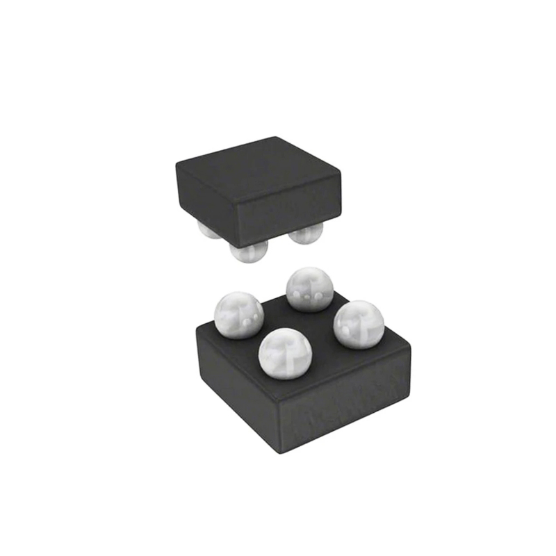
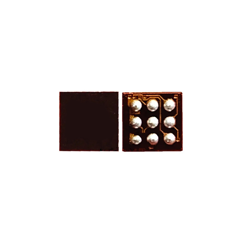
Bilder dienen nur zur Referenz. Siehe Produktspezifikationen.
Bestellungen über
$5000Microchip PM8056B-FEI
Interface - I/O Expanders SXP 68x12G


Marken: Microchip Technology, Inc
Herstellerteil #: PM8056B-FEI
Datenblatt: PM8056B-FEI Datasheet (PDF)
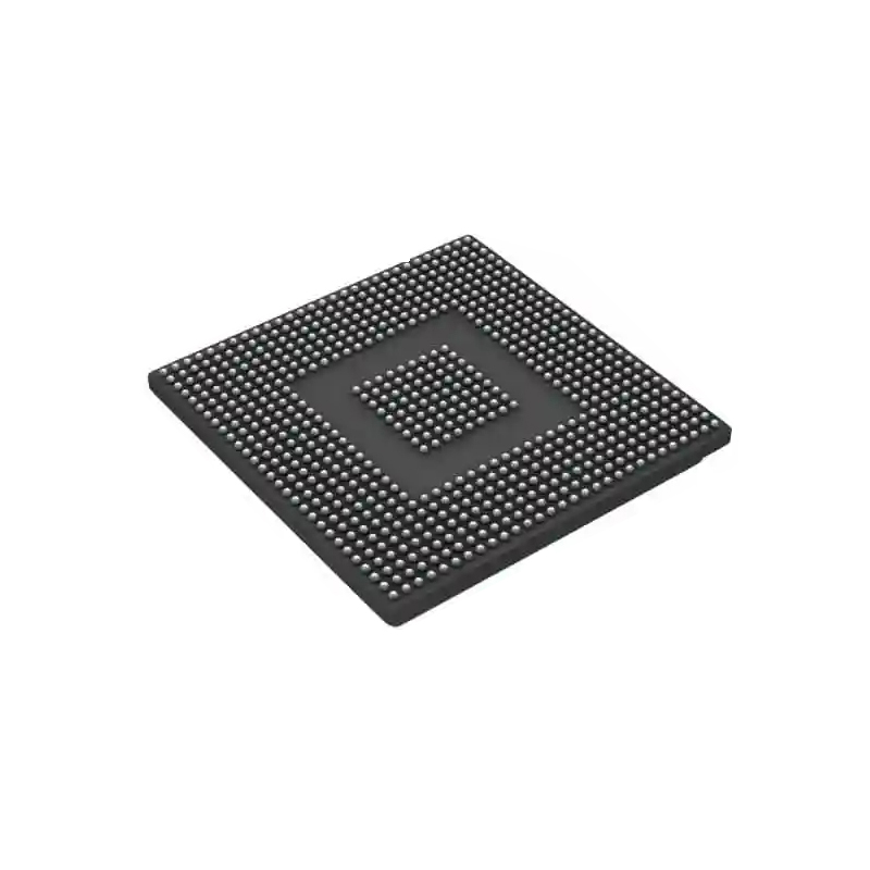
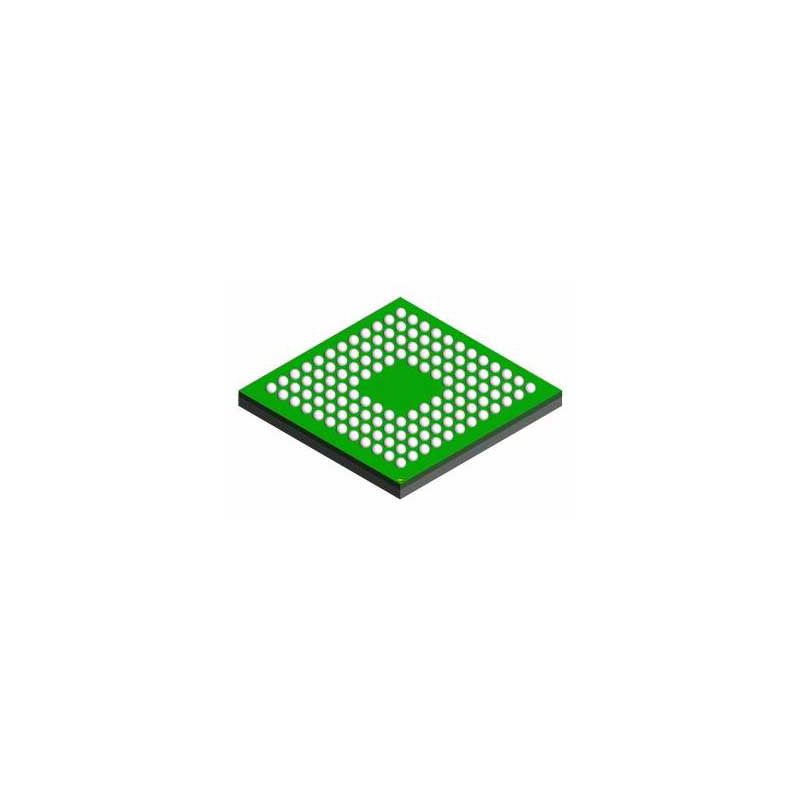
Paket/Gehäuse: BFBGA
Produktart: I/O Expanders
RoHS-Status:
Lagerzustand: 2.957 Stück, Neues Original
Warranty: 1 Year Ovaga Warranty - Find Out More
0
1
Funktionen
- SAS-3 T10 zoning for secure storage
- Ultra low switching latency for improved system performance
- SAS and SATA edge-buffering preserves customers’ investment by improving performance with existing 3G and 6G drives
- Table-to-table routing removes need for keyed connectors
- Integrated Ethernet port for seamless interface to management entity
- Integrated MIPS processor for enclosure management
- Firmware compatible with Microchip SAS 3 Gbps and 6 Gbps SAS expanders and stand-alone enclosure management controllers
- 12G SAS signaling support for up to 10m mini-SAS HD passive copper cable
- Optical SAS support
- Early power off warning (EPOW) support
- SAS and SATA edge-buffering support
- Ultra-low switching latency to improve system performance
- Quad SPI or parallel flash support; optional inline ECC on the parallel flash
- T10 zoning support (up to 256 zones)
- Port mirroring for system debug
- Local bus data integrity protection
- Real-time eye capture with enhanced BER eye mask and estimation
- Non-disruptive zero down time firmware update support
- Position-independent firmware image support to simplify firmware image management/download
- Compatible enclosure management firmware architecture with SXP 3G/6G products
- Real-time clock (1 µS counter up to 35+ years)
- Enhanced processing subsystem (MIPS 34Kc at 600 MHz)
- Backward-compatibility with Microchii’s 6G/3G SXP devices
- High-Speed I/O
- SAS-3 (12 Gbps, 6 Gbps, 3 Gbps, 1.5 Gbps) and SATA-3 (6 Gbps, 3 Gbps, 1.5 Gbps) operation
- Support for up to 4K SAS addresses
- Automated decision feedback equalizer (DFE) per SAS-3
- Programmable continuous time linear equalizer for SATA-3
- Supports spread-spectrum clocking (SSC) per SAS/SATA-3
- Per-PHY configurable transmit and receive SSC
- Per-PHY programmable transmit amplitude and emphasis
- Integrated resistive termination
- SAS 3.0-compliant back-channel training (SAS3 speed negotiation)
- Peripheral Interfaces
- 4 UART interfaces for system monitoring and debugging
- 4 SGPIO interfaces (or additional TWI per SFF-8448)
- Up to 81 GPIO pins
- Eight dedicated two-wire interfaces (up to twelve total) for device configuration and control of external interfaces
- 16-bit local bus interface for connecting to NOR flash and SRAM
- SPI, DSPI, and QSPI interface
- 10/100 Ethernet MAC port
- JTAG and EJTAG interface
- Statistics and Performance Monitoring
- Per-port error counters for comprehensive diagnostic capability
- Programmable PMON counters and interrupt generation
- Per-link PRBS and CJPAT pattern generators and loop-backs for linkintegrity diagnostics
- Real-time clock
- Firmware Development Kit
- Zoning configuration interface
- SAM4/SPC4/SES3-compatible SES target with Enclosure Management Application reference design
- SAS-3-compatible protocol stack in virtual SAS/SMP port
- SSP/STP Initiator API supports communication with SSP/STP targets over SAS links
- SMP routing management including topology discovery
- Firmware download over multiple in-band and out-of-band interfaces
- Expander diagnostics API
- Disk spin-up control and disk qualification API
- Peripheral drivers for TWI, UART, SGPIO, and Ethernet interfaces
- TCP/IP enables management of the SXP 12G through remote network
- Error detection, logging, and reporting
- Wake up system through Ethernet or SAS port
- Chiplink Diagnostic Utility
- Supports advanced features for validation, characterization and debugging of Microchip expanders
- Includes full SAS tool suite and a macro interface for user-authored animation scripts
- Third Party Support
- Green Hills MULTI development environment and EJTAG debugger
- SAS-3 (12 Gbps, 6 Gbps, 3 Gbps, 1.5 Gbps) and SATA-3 (6 Gbps, 3 Gbps, 1.5 Gbps) operation
- Support for up to 4K SAS addresses
- Automated decision feedback equalizer (DFE) per SAS-3
- Programmable continuous time linear equalizer for SATA-3
- Supports spread-spectrum clocking (SSC) per SAS/SATA-3
- Per-PHY configurable transmit and receive SSC
- Per-PHY programmable transmit amplitude and emphasis
- Integrated resistive termination
- SAS 3.0-compliant back-channel training (SAS3 speed negotiation)
- 4 UART interfaces for system monitoring and debugging
- 4 SGPIO interfaces (or additional TWI per SFF-8448)
- Up to 81 GPIO pins
- Eight dedicated two-wire interfaces (up to twelve total) for device configuration and control of external interfaces
- 16-bit local bus interface for connecting to NOR flash and SRAM
- SPI, DSPI, and QSPI interface
- 10/100 Ethernet MAC port
- JTAG and EJTAG interface
- Per-port error counters for comprehensive diagnostic capability
- Programmable PMON counters and interrupt generation
- Per-link PRBS and CJPAT pattern generators and loop-backs for linkintegrity diagnostics
- Real-time clock
- Zoning configuration interface
- SAM4/SPC4/SES3-compatible SES target with Enclosure Management Application reference design
- SAS-3-compatible protocol stack in virtual SAS/SMP port
- SSP/STP Initiator API supports communication with SSP/STP targets over SAS links
- SMP routing management including topology discovery
- Firmware download over multiple in-band and out-of-band interfaces
- Expander diagnostics API
- Disk spin-up control and disk qualification API
- Peripheral drivers for TWI, UART, SGPIO, and Ethernet interfaces
- TCP/IP enables management of the SXP 12G through remote network
- Error detection, logging, and reporting
- Wake up system through Ethernet or SAS port
- Supports advanced features for validation, characterization and debugging of Microchip expanders
- Includes full SAS tool suite and a macro interface for user-authored animation scripts
- Green Hills MULTI development environment and EJTAG debugger

Spezifikationen
| Parameter | Wert | Parameter | Wert |
|---|---|---|---|
| feature-process-technology | feature-minimum-operating-supply-voltage-v | ||
| feature-maximum-operating-supply-voltage-v | feature-packaging | ||
| feature-rad-hard | feature-pin-count | ||
| feature-supplier-package | feature-standard-package-name1 | ||
| feature-cecc-qualified | feature-esd-protection | ||
| feature-escc-qualified | feature-military | ||
| feature-aec-qualified | feature-aec-qualified-number | ||
| feature-auto-motive | feature-p-pap | ||
| feature-eccn-code | EAR99 | feature-svhc | Yes |
| feature-svhc-exceeds-threshold | No |
Versand
| Versandart | Versandgebühr | Vorlaufzeit | |
|---|---|---|---|
 |
DHL | $20.00-$40.00 (0.50 KG) | 2-5 Tage |
 |
FedEx | $20.00-$40.00 (0.50 KG) | 2-5 Tage |
 |
UPS | $20.00-$40.00 (0.50 KG) | 2-5 Tage |
 |
TNT | $20.00-$40.00 (0.50 KG) | 2-5 Tage |
 |
EMS | $20.00-$40.00 (0.50 KG) | 2-5 Tage |
 |
REGISTRIERTE LUFTPOST | $20.00-$40.00 (0.50 KG) | 2-5 Tage |
Bearbeitungszeit: Die Versandkosten hängen von der jeweiligen Zone und dem Land ab.
Zahlung
| Zahlungsbedingungen | Handgebühr | |
|---|---|---|
 |
Banküberweisung | Bankgebühr in Höhe von 30,00 USD wird berechnet. |
 |
Paypal | 4,0 % Servicegebühr wird berechnet. |
 |
Kreditkarte | 3,5 % Servicegebühr wird berechnet. |
 |
Western Union | charge US.00 banking fee. |
 |
Geldgramm | Bankgebühr in Höhe von 0,00 USD wird berechnet. |
Garantien
1. Die von Ihnen gekauften elektronischen Bauteile enthalten eine 365-tägige Garantie. Wir garantieren die Produktqualität.
2. Wenn einige der Artikel, die Sie erhalten haben, nicht von perfekter Qualität sind, würden wir verantwortungsvoll Ihre Rückerstattung oder Ersatz arrangieren. Die Artikel müssen jedoch in ihrem Originalzustand verbleiben.
Verpackung
-

Schritt1 :Produkt
-

Schritt2 :Vakuumverpackung
-

Schritt3 :Antistatikbeutel
-

Schritt4 :Individuelle Verpackung
-

Schritt5 :Verpackungskartons
-

Schritt6 :Barcode-Versandetikett


Alle Produkte werden in antistatischen Beuteln verpackt. Versand mit ESD-Antistatikschutz.
Auf dem äußeren ESD-Verpackungsetikett werden die Informationen unseres Unternehmens verwendet: Teilenummer, Marke und Menge.
Wir prüfen alle Waren vor dem Versand, stellen sicher, dass sich alle Produkte in gutem Zustand befinden und dass die Teile neu und original sind und mit dem Datenblatt übereinstimmen.
Nachdem alle Waren darauf überprüft wurden, dass nach dem Verpacken keine Probleme auftreten, werden wir sicher verpacken und per Global Express versenden. Es zeigt eine ausgezeichnete Durchstoß- und Reißfestigkeit sowie eine gute Dichtungsintegrität.


Teilpunkte
-
The PM8056B-FEI is a 5G system-on-a-chip (SoC) developed by Qualcomm for mobile devices. It offers advanced connectivity, power efficiency, and performance for a seamless user experience. The chip integrates multiple components such as a modem, processor, and AI engine, making it an ideal solution for high-speed data transfer and multimedia applications.
-
Equivalent
Equivalent products of PM8056B-FEI chip include Qualcomm Snapdragon 835, MediaTek Helio P60, and Samsung Exynos 8895. These chips are similar in performance and features, making them suitable alternatives for various electronic devices. -
Features
The PM8056B-FEI is a high-frequency, energy-efficient integrated circuit designed for power management applications. It features a wide input voltage range, low dropout voltage, high efficiency, integrated voltage regulation, and thermal protection. Its small form factor makes it ideal for compact electronic devices. -
Pinout
The PM8056B-FEI is a power management integrated circuit with a 226-pin count. It includes functions such as voltage regulation, power sequencing, and battery charging for mobile devices. -
Manufacturer
PM8056B-FEI is manufactured by QUALCOMM Technologies, Inc. It is a leading semiconductor and telecommunications equipment company known for producing wireless communication technologies, including processors, modems, and chips for smartphones, IoT devices, and other electronic devices. -
Application Field
PM8056B-FEI is used in various applications such as network infrastructure, telecommunications, industrial automation, and military and aerospace systems. It provides advanced functionalities like low-power consumption, high-performance processing, and secure communication capabilities, making it ideal for a wide range of high-demanding applications. -
Package
The PM8056B-FEI chip is a BGA (Ball Grid Array) package with a form factor size of 11.5mm x 11.5mm.


Datenblatt PDF
Wir bieten qualitativ hochwertige Produkte, durchdachten Service und eine Kundendienstgarantie
-

Wir haben reichhaltige Produkte, die Ihre unterschiedlichen Bedürfnisse erfüllen können.
-

Die Mindestbestellmenge beginnt bei 1 Stück.
-

Niedrigste internationale Versandgebühr beginnt ab 0,00 USD
-

365 Tage Qualitätsgarantie für alle Produkte


Ovaga stands out for their professionalism and quality.