Bilder dienen nur zur Referenz. Siehe Produktspezifikationen.
Bestellungen über
$5000A3P060-TQG144
0000 Gates, 1536 CLBs, 350MHz, Field Programmable Gate Array, CMOS, PQFP144


Marken: MICROCHIP TECHNOLOGY INC
Herstellerteil #: A3P060-TQG144
Datenblatt: A3P060-TQG144 Datenblatt (PDF)
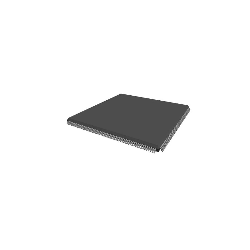
Paket/Gehäuse: TQFP-144
Produktart: FPGAs (Field Programmable Gate Array)
RoHS-Status:
Lagerzustand: 8.407 Stück, Neues Original
Warranty: 1 Year Ovaga Warranty - Find Out More
0
1
A3P060-TQG144 Allgemeine Beschreibung
Suitable for a variety of applications, the A3P060-TQG144 FPGA from Microchip Technology is part of the ProASIC3 family and comes in a TQG144 package. With 60,000 System Gates, 2880 Logic Cells, and 72 I/Os, this FPGA offers flexibility and customization for complex digital systems. Its 1 Mbit of embedded Flash memory eliminates the need for external memory components, reducing overall system cost. Operating at a maximum frequency of 250 MHz, the A3P060-TQG144 delivers high-speed performance for demanding applications
Funktionen
High Capacity 15 k to 1 M System Gates Up to 144 kbits of True Dual-Port SRAM Up to 300 User I/OsReprogrammable Flash Technology 130-nm, 7-Layer Metal (6 Copper), Flash-Based CMOS Process Instant On Level 0 Support Single-Chip Solution Retains Programmed Design when Powered OffHigh Performance 350 MHz System Performance 3.3 V, 66 MHz 64-Bit PCIIn-System Programming (ISP) and Security ISP Using On-Chip 128-Bit Advanced Encryption Standard (AES) Decryption (except ARM-enabled ProASIC3 devices) via JTAG (IEEE 1532compliant) FlashLock to Secure FPGA ContentsLow Power Core Voltage for Low Power Support for 1.5 V-Only Systems Low-Impedance Flash SwitchesHigh-Performance Routing Hierarchy Segmented, Hierarchical Routing and Clock StructureAdvanced I/O 700 Mbps DDR, LVDS-Capable I/Os (A3P250 and above) 1.5 V, 1.8 V, 2.5 V, and 3.3 V Mixed-Voltage Operation Wide Range Power Supply Voltage Support per JESD8-B, Allowing I/Os to Operate from 2.7 V to 3.6 V Bank-Selectable I/O Voltagesup to 4 Banks per Chip Single-Ended I/O Standards: LVTTL, LVCMOS 3.3 V / 2.5 V / 1.8 V / 1.5 V, 3.3 V PCI / 3.3 V PCI-X and LVCMOS 2.5 V / 5.0 V Input Differential I/O Standards: LVPECL, LVDS, B-LVDS, and M-LVDS (A3P250 and above) I/O Registers on Input, Output, and Enable Paths Hot-Swappable and Cold Sparing I/Os Programmable Output Slew Rate and Drive Strength Weak Pull-Up/-Down IEEE 1149.1 (JTAG) Boundary Scan Test Pin-Compatible Packages across the ProASIC3 FamilyClock Conditioning Circuit (CCC) and PLL Six CCC Blocks, One with an Integrated PLL Configurable Phase-Shift, Multiply/Divide, Delay Capabilities and External Feedback Wide Input Frequency Range (1.5 MHz to 350 MHz)Embedded Memory 1 kbit of FlashROM User Nonvolatile Memory SRAMs and FIFOs with Variable-Aspect-Ratio 4,608-Bit RAM Blocks (1, 2, 4, 9, and 18 organizations) True Dual-Port SRAM (except 18)ARM Processor Support in ProASIC3 FPGAs M1 ProASIC3 DevicesARMCortex-M1 Soft Processor Available with or without Debug
Spezifikationen
| Parameter | Wert | Parameter | Wert |
|---|---|---|---|
| Rohs Code | Yes | Part Life Cycle Code | Active |
| Ihs Manufacturer | MICROCHIP TECHNOLOGY INC | Package Description | 20 X 20 MM, 1.40 MM HEIGHT, 0.50 MM PITCH, GREEN, TQFP-144 |
| Reach Compliance Code | compliant | HTS Code | 8542.39.00.01 |
| Factory Lead Time | 52 Weeks | Clock Frequency-Max | 350 MHz |
| JESD-30 Code | S-PQFP-G144 | JESD-609 Code | e3 |
| Length | 20 mm | Moisture Sensitivity Level | 3 |
| Number of CLBs | 1536 | Number of Equivalent Gates | 60000 |
| Number of Terminals | 144 | Operating Temperature-Max | 85 °C |
| Operating Temperature-Min | Organization | 1536 CLBS, 60000 GATES | |
| Package Body Material | PLASTIC/EPOXY | Package Code | LFQFP |
| Package Shape | SQUARE | Package Style | FLATPACK, LOW PROFILE, FINE PITCH |
| Programmable Logic Type | FIELD PROGRAMMABLE GATE ARRAY | Qualification Status | Not Qualified |
| Seated Height-Max | 1.6 mm | Supply Voltage-Max | 1.575 V |
| Supply Voltage-Min | 1.425 V | Supply Voltage-Nom | 1.5 V |
| Surface Mount | YES | Technology | CMOS |
| Temperature Grade | COMMERCIAL | Terminal Finish | MATTE TIN |
| Terminal Form | GULL WING | Terminal Pitch | 0.5 mm |
| Terminal Position | QUAD |
Versand
| Versandart | Versandgebühr | Vorlaufzeit | |
|---|---|---|---|
 |
DHL | $20.00-$40.00 (0.50 KG) | 2-5 Tage |
 |
FedEx | $20.00-$40.00 (0.50 KG) | 2-5 Tage |
 |
UPS | $20.00-$40.00 (0.50 KG) | 2-5 Tage |
 |
TNT | $20.00-$40.00 (0.50 KG) | 2-5 Tage |
 |
EMS | $20.00-$40.00 (0.50 KG) | 2-5 Tage |
 |
REGISTRIERTE LUFTPOST | $20.00-$40.00 (0.50 KG) | 2-5 Tage |
Bearbeitungszeit: Die Versandkosten hängen von der jeweiligen Zone und dem Land ab.
Zahlung
| Zahlungsbedingungen | Handgebühr | |
|---|---|---|
 |
Banküberweisung | Bankgebühr in Höhe von 30,00 USD wird berechnet. |
 |
Paypal | 4,0 % Servicegebühr wird berechnet. |
 |
Kreditkarte | 3,5 % Servicegebühr wird berechnet. |
 |
Western Union | charge US.00 banking fee. |
 |
Geldgramm | Bankgebühr in Höhe von 0,00 USD wird berechnet. |
Garantien
1. Die von Ihnen gekauften elektronischen Bauteile enthalten eine 365-tägige Garantie. Wir garantieren die Produktqualität.
2. Wenn einige der Artikel, die Sie erhalten haben, nicht von perfekter Qualität sind, würden wir verantwortungsvoll Ihre Rückerstattung oder Ersatz arrangieren. Die Artikel müssen jedoch in ihrem Originalzustand verbleiben.
Verpackung
-

Schritt1 :Produkt
-

Schritt2 :Vakuumverpackung
-

Schritt3 :Antistatikbeutel
-

Schritt4 :Individuelle Verpackung
-

Schritt5 :Verpackungskartons
-

Schritt6 :Barcode-Versandetikett


Alle Produkte werden in antistatischen Beuteln verpackt. Versand mit ESD-Antistatikschutz.
Auf dem äußeren ESD-Verpackungsetikett werden die Informationen unseres Unternehmens verwendet: Teilenummer, Marke und Menge.
Wir prüfen alle Waren vor dem Versand, stellen sicher, dass sich alle Produkte in gutem Zustand befinden und dass die Teile neu und original sind und mit dem Datenblatt übereinstimmen.
Nachdem alle Waren darauf überprüft wurden, dass nach dem Verpacken keine Probleme auftreten, werden wir sicher verpacken und per Global Express versenden. Es zeigt eine ausgezeichnete Durchstoß- und Reißfestigkeit sowie eine gute Dichtungsintegrität.


Teilpunkte
-
The A3P060-TQG144 chip is a programmable logic device (PLD) from Actel/Microsemi that features 60,000 system gates and is housed in a 144-pin TQFP package. It offers a low-power, high-performance solution for a wide range of applications, including industrial automation, telecommunications, and consumer electronics.
-
Equivalent
Some equivalent products of the A3P060-TQG144 chip are XA3P060, A3P030, A3P060, A3P060-2VQG100, A3P060-2VQ100, and A3P060-2TQG144. These are all similar in terms of functionality, performance, and compatibility with different hardware and software systems. -
Features
A3P060-TQG144 is a flash-based, low power, and high reliability FPGA device. It offers 60,000 system gates with 144-pin TQFP package, and features FlashLock security, JTAG boundary scan, and programmable power management. It is suitable for a wide range of applications in industrial, automotive, and consumer markets. -
Pinout
A3P060-TQG144 is a flash-based FPGA with 144-pin TQFP package. It has 60 user I/O pins, along with various power, ground, and configuration pins. The function includes programmable logic functions, on-chip flash memory, and embedded 6051 processor core. -
Manufacturer
A3P060-TQG144 is manufactured by Microsemi Corporation, which is a leading provider of semiconductor solutions specializing in aerospace, defense, communications, and industrial markets. The company designs and produces high-performance and reliable integrated circuits for a wide range of applications, including FPGAs like the A3P060-TQG144. -
Application Field
A3P060-TQG144 is commonly used in various application areas such as industrial automation, automotive systems, telecommunications, and consumer electronics. It is ideal for applications requiring low power consumption, high performance, and compact size. This programmable logic device can be used for signal processing, motor control, data acquisition, and communication interfaces. -
Package
The A3P060-TQG144 chip has a Thin Quad Flat Pack (TQFP) package, with a form factor of 144 pins and a size of 14mm x 14mm.


Wir bieten qualitativ hochwertige Produkte, durchdachten Service und eine Kundendienstgarantie
-

Wir haben reichhaltige Produkte, die Ihre unterschiedlichen Bedürfnisse erfüllen können.
-

Die Mindestbestellmenge beginnt bei 1 Stück.
-

Niedrigste internationale Versandgebühr beginnt ab 0,00 USD
-

365 Tage Qualitätsgarantie für alle Produkte