

Bilder dienen nur zur Referenz. Siehe Produktspezifikationen.
Bestellungen über
$5000
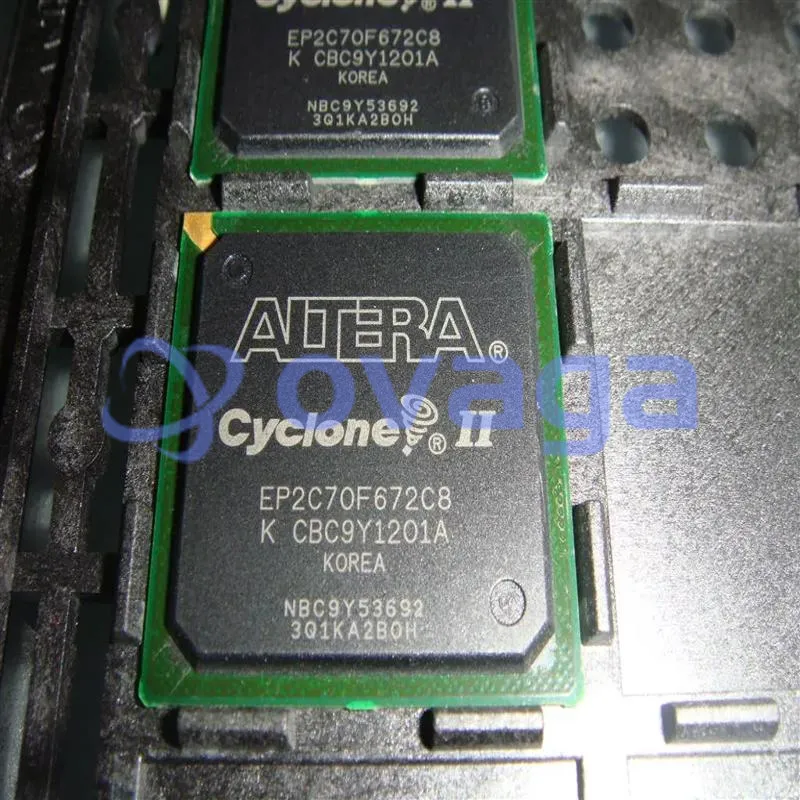
Intel EP2C70F672C8

ROHS Compliant EP2C70F672C8 68416 4276 FBGA-672(27x27) Programmable Logic Device


Marken: INTEL CORP
Herstellerteil #: EP2C70F672C8
Datenblatt: EP2C70F672C8 Datenblatt (PDF)
Paket/Gehäuse: FBGA-672
RoHS-Status:
Lagerzustand: 6.554 Stück, Neues Original
Produktart: FPGAs (Field Programmable Gate Array)
Warranty: 1 Year Ovaga Warranty - Find Out More
0
1
*Alle Preise sind in USD
| Menge | Einzelpreis | Ext. Preis |
|---|---|---|
| 1 | $1408,287 | $1408,287 |
| 200 | $561,916 | $112383,200 |
| 480 | $543,139 | $260706,720 |
| 1000 | $533,860 | $533860,000 |
Auf Lager: 6.554 Stck
EP2C70F672C8 Allgemeine Beschreibung
In conclusion, the EP2C70F672C8 FPGA from Intel (formerly Altera) stands as a reliable and efficient solution for complex digital designs. With its high logic element count, embedded memory, dedicated multipliers, and various I/O options, this FPGA is well-suited for a wide range of applications in telecommunications, automotive, industrial control, and more. Its support for Intel's Quartus Prime development software further enhances its usability, making it a valuable tool for engineers and designers working on advanced projects
Funktionen
- High-density architecture with 4,608 to 68,416 LEs
- M4K embedded memory blocks
- Up to 1.1 Mbits of RAM available without reducing available logic
- 4,096 memory bits per block (4,608 bits per block including 512 parity bits)
- Variable port configurations of ×1, ×2, ×4, ×8, ×9, ×16, ×18, ×32, and ×36
- True dual-port (one read and one write, two reads, or two writes) operation for ×1, ×2, ×4, ×8, ×9, ×16, and ×18 modes
- Byte enables for data input masking during writes
- Up to 260-MHz operation
- Embedded multipliers
- Up to 150 18- × 18-bit multipliers are each configurable as two independent 9- × 9-bit multipliers with up to 250-MHz performance
- Optional input and output registers
- Advanced I/O support
- High-speed differential I/O standard support, including LVDS, RSDS, mini-LVDS, LVPECL, differential HSTL, and differential SSTL
- Single-ended I/O standard support, including 2.5-V and 1.8-V, SSTL class I and II, 1.8-V and 1.5-V HSTL class I and II, 3.3-V PCI and PCI-X 1.0, 3.3-, 2.5-, 1.8-, and 1.5-V LVCMOS, and 3.3-, 2.5-, and 1.8-V LVTTL
- Peripheral Component Interconnect Special Interest Group (PCI SIG) PCI Local Bus Specification, Revision 3.0 compliance for 3.3-V operation at 33 or 66 MHz for 32- or 64-bit interfaces
- PCI Express with an external TI PHY and an Altera PCI Express ×1 Megacore® function
- 133-MHz PCI-X 1.0 specification compatibility
- High-speed external memory support, including DDR, DDR2, and SDR SDRAM, and QDRII SRAM supported by drop in Altera IP MegaCore functions for ease of use
- Three dedicated registers per I/O element (IOE): one input register, one output register, and one output-enable register
- Programmable bus-hold feature
- Programmable output drive strength feature
- Programmable delays from the pin to the IOE or logic array
- I/O bank grouping for unique VCCIO and/or VREF bank settings
- MultiVolt™ I/O standard support for 1.5-, 1.8-, 2.5-, and 3.3-interfaces
- Hot-socketing operation support
- Tri-state with weak pull-up on I/O pins before and during configuration
- Programmable open-drain outputs
- Series on-chip termination support
- (Continue .)

Spezifikationen
| Parameter | Wert | Parameter | Wert |
|---|---|---|---|
| Rohs Code | No | Part Life Cycle Code | Active |
| Ihs Manufacturer | INTEL CORP | Package Description | FBGA-672 |
| Reach Compliance Code | compliant | HTS Code | 8542.39.00.01 |
| Additional Feature | ALSO REQUIRES 3.3 SUPPLY | Clock Frequency-Max | 402.5 MHz |
| JESD-30 Code | S-PBGA-B672 | JESD-609 Code | e0 |
| Length | 27 mm | Moisture Sensitivity Level | 3 |
| Number of CLBs | 4276 | Number of Inputs | 422 |
| Number of Logic Cells | 68416 | Number of Outputs | 406 |
| Number of Terminals | 672 | Operating Temperature-Max | 85 °C |
| Operating Temperature-Min | Organization | 4276 CLBS | |
| Package Body Material | PLASTIC/EPOXY | Package Code | BGA |
| Package Equivalence Code | BGA672,26X26,40 | Package Shape | SQUARE |
| Package Style | GRID ARRAY | Power Supplies | 1.2,1.5/3.3,3.3 V |
| Programmable Logic Type | FIELD PROGRAMMABLE GATE ARRAY | Qualification Status | Not Qualified |
| Seated Height-Max | 2.6 mm | Supply Voltage-Max | 1.25 V |
| Supply Voltage-Min | 1.15 V | Supply Voltage-Nom | 1.2 V |
| Surface Mount | YES | Technology | CMOS |
| Temperature Grade | OTHER | Terminal Finish | TIN LEAD |
| Terminal Form | BALL | Terminal Pitch | 1 mm |
| Terminal Position | BOTTOM |
Versand
| Versandart | Versandgebühr | Vorlaufzeit | |
|---|---|---|---|
 |
DHL | $20.00-$40.00 (0.50 KG) | 2-5 Tage |
 |
FedEx | $20.00-$40.00 (0.50 KG) | 2-5 Tage |
 |
UPS | $20.00-$40.00 (0.50 KG) | 2-5 Tage |
 |
TNT | $20.00-$40.00 (0.50 KG) | 2-5 Tage |
 |
EMS | $20.00-$40.00 (0.50 KG) | 2-5 Tage |
 |
REGISTRIERTE LUFTPOST | $20.00-$40.00 (0.50 KG) | 2-5 Tage |
Bearbeitungszeit: Die Versandkosten hängen von der jeweiligen Zone und dem Land ab.
Zahlung
| Zahlungsbedingungen | Handgebühr | |
|---|---|---|
 |
Banküberweisung | Bankgebühr in Höhe von 30,00 USD wird berechnet. |
 |
Paypal | 4,0 % Servicegebühr wird berechnet. |
 |
Kreditkarte | 3,5 % Servicegebühr wird berechnet. |
 |
Western Union | charge US.00 banking fee. |
 |
Geldgramm | Bankgebühr in Höhe von 0,00 USD wird berechnet. |
Garantien
1. Die von Ihnen gekauften elektronischen Bauteile enthalten eine 365-tägige Garantie. Wir garantieren die Produktqualität.
2. Wenn einige der Artikel, die Sie erhalten haben, nicht von perfekter Qualität sind, würden wir verantwortungsvoll Ihre Rückerstattung oder Ersatz arrangieren. Die Artikel müssen jedoch in ihrem Originalzustand verbleiben.
Verpackung
-

Schritt1 :Produkt
-

Schritt2 :Vakuumverpackung
-

Schritt3 :Antistatikbeutel
-

Schritt4 :Individuelle Verpackung
-

Schritt5 :Verpackungskartons
-

Schritt6 :Barcode-Versandetikett


Alle Produkte werden in antistatischen Beuteln verpackt. Versand mit ESD-Antistatikschutz.
Auf dem äußeren ESD-Verpackungsetikett werden die Informationen unseres Unternehmens verwendet: Teilenummer, Marke und Menge.
Wir prüfen alle Waren vor dem Versand, stellen sicher, dass sich alle Produkte in gutem Zustand befinden und dass die Teile neu und original sind und mit dem Datenblatt übereinstimmen.
Nachdem alle Waren darauf überprüft wurden, dass nach dem Verpacken keine Probleme auftreten, werden wir sicher verpacken und per Global Express versenden. Es zeigt eine ausgezeichnete Durchstoß- und Reißfestigkeit sowie eine gute Dichtungsintegrität.


Teilpunkte
-
The EP2C70F672C8 is a field-programmable gate array (FPGA) chip manufactured by Intel. It belongs to the Cyclone II family and features 70,000 logic elements, 622 user I/O pins, and 504 embedded multipliers. With its configurable nature, it's widely used in various applications such as telecommunications, industrial automation, and consumer electronics.
-
Equivalent
The EP2C70F672C8 chip is part of Altera's Cyclone II FPGA series. Equivalent products include Xilinx's Spartan-3, Lattice Semiconductor's MachXO2, and Microchip's SmartFusion2. Each offers similar programmable logic capabilities, though specifics may vary. -
Features
The EP2C70F672C8 is an Altera Cyclone II FPGA. Its features include 70,000 logic elements, 4 Mbits of embedded memory, 266 MHz maximum core frequency, and 672 user I/O pins. It operates on a 1.2V core voltage and supports various communication protocols like PCIe and Gigabit Ethernet. -
Pinout
The EP2C70F672C8 is an FPGA with 672 pins. Its functions include programmable logic, configurable I/Os, memory blocks, and DSP slices for flexible customization and high-performance computing tasks. -
Manufacturer
The EP2C70F672C8 is manufactured by Altera Corporation, now part of Intel Corporation. Altera specialized in manufacturing programmable logic devices, particularly field-programmable gate arrays (FPGAs). FPGAs are integrated circuits designed to be configured by a customer or a designer after manufacturing, allowing for customizable hardware solutions in various applications like telecommunications, automotive, and industrial automation. -
Application Field
The EP2C70F672C8 is commonly used in a variety of applications, including telecommunications, industrial automation, automotive, and aerospace. It is suitable for applications that require high-performance processing, reliable operation, and low power consumption. Its FPGA architecture allows for flexibility and adaptability in a range of different environments. -
Package
The EP2C70F672C8 chip is a Field-Programmable Gate Array (FPGA) from Intel (formerly Altera). It comes in a Ball Grid Array (BGA) package with a form factor of 672-pin. The package size is 27mm x 27mm.


Wir bieten qualitativ hochwertige Produkte, durchdachten Service und eine Kundendienstgarantie
-

Wir haben reichhaltige Produkte, die Ihre unterschiedlichen Bedürfnisse erfüllen können.
-

Die Mindestbestellmenge beginnt bei 1 Stück.
-

Niedrigste internationale Versandgebühr beginnt ab 0,00 USD
-

365 Tage Qualitätsgarantie für alle Produkte


