


Bilder dienen nur zur Referenz. Siehe Produktspezifikationen.
Bestellungen über
$5000
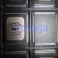
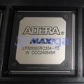
Altera EP2C70F896C6N

With 896 pins and housed in a fine-pitch ball grid array (FBGA) package


Marken: Altera
Herstellerteil #: EP2C70F896C6N
Datenblatt: EP2C70F896C6N Datenblatt (PDF)
Paket/Gehäuse: FBGA-896
RoHS-Status:
Lagerzustand: 2.399 Stück, Neues Original
Produktart: FPGAs (Field Programmable Gate Array)
Warranty: 1 Year Ovaga Warranty - Find Out More
0
1
*Alle Preise sind in USD
| Menge | Einzelpreis | Ext. Preis |
|---|---|---|
| 1 | $2090,893 | $2090,893 |
| 189 | $834,280 | $157678,920 |
| 513 | $806,402 | $413684,226 |
| 999 | $792,626 | $791833,374 |
Auf Lager: 2.399 Stck
EP2C70F896C6N Allgemeine Beschreibung
The EP2C70F896C6N FPGA, a cornerstone of Altera's legacy now seamlessly integrated into Intel's portfolio, is a testament to relentless innovation in the realm of programmable logic devices. Boasting a formidable arsenal of 70,000 logic elements and 896 pins, it stands as a pinnacle of engineering prowess, designed to excel in mission-critical applications demanding both speed and efficiency. With its finely tuned architecture and comprehensive feature set—including embedded memory, DSP slices, and PLLs—it delivers unparalleled performance across diverse domains. Whether deployed in telecommunications infrastructure or automotive control systems, its adaptability and reconfigurability empower developers to push the boundaries of what's possible, ushering in a new era of computational agility and efficiency

Spezifikationen
| Parameter | Wert | Parameter | Wert |
|---|---|---|---|
| feature-family-name | Cyclone® II | feature-process-technology | 90nm |
| feature-maximum-number-of-user-i-os | 622 | feature-number-of-registers | |
| feature-device-logic-cells | 68416 | feature-device-system-gates | |
| feature-number-of-multipliers | 150 (18x18) | feature-program-memory-type | SRAM |
| feature-ram-bits-kbit | 1125 | feature-total-number-of-block-ram | 250 |
| feature-ethernet-macs | feature-supported-ip-core | 32/64-bit PCI-X bus Master/Target interface Core, 66/100/133Mhz|10 Gigabit Ethernet MAC|SpeedView Enabled JPEG Encoder (SVE-JPEG-E)|V1 ColdFire|Viterbi Compiler, Low-Speed/Hybrid Serial Decoder | |
| feature-supported-ip-core-manufacture | Altera/Freescale/CAST, Inc/MorethanIP/PLDA | feature-maximum-number-of-serdes-channels | |
| feature-device-logic-units | 68416 | feature-device-number-of-dlls-plls | 4 |
| feature-transceiver-blocks | feature-transceiver-speed-gbps | ||
| feature-dedicated-dsp | feature-pci-blocks | ||
| feature-programmability | No | feature-maximum-internal-frequency-mhz | 500 |
| feature-speed-grade | 6 | feature-giga-multiply-accumulates-per-second | |
| feature-differential-i-o-standards-supported | PCI-X|LVDS | feature-single-ended-i-o-standards-supported | PCI-X|LVDS |
| feature-external-memory-interface | QDR II+SRAM|DDR SDRAM | feature-minimum-operating-supply-voltage-v | 1.15 |
| feature-maximum-operating-supply-voltage-v | 1.25 | feature-packaging | |
| feature-rohs | feature-rad-hard | ||
| feature-pin-count | 896 | feature-supplier-package | FBGA |
| feature-standard-package-name1 | BGA | feature-cecc-qualified | No |
| feature-esd-protection | feature-escc-qualified | ||
| feature-military | No | feature-aec-qualified | No |
| feature-aec-qualified-number | feature-auto-motive | No | |
| feature-p-pap | No | feature-eccn-code | 3A991 |
| feature-svhc | No |
Versand
| Versandart | Versandgebühr | Vorlaufzeit | |
|---|---|---|---|
 |
DHL | $20.00-$40.00 (0.50 KG) | 2-5 Tage |
 |
FedEx | $20.00-$40.00 (0.50 KG) | 2-5 Tage |
 |
UPS | $20.00-$40.00 (0.50 KG) | 2-5 Tage |
 |
TNT | $20.00-$40.00 (0.50 KG) | 2-5 Tage |
 |
EMS | $20.00-$40.00 (0.50 KG) | 2-5 Tage |
 |
REGISTRIERTE LUFTPOST | $20.00-$40.00 (0.50 KG) | 2-5 Tage |
Bearbeitungszeit: Die Versandkosten hängen von der jeweiligen Zone und dem Land ab.
Zahlung
| Zahlungsbedingungen | Handgebühr | |
|---|---|---|
 |
Banküberweisung | Bankgebühr in Höhe von 30,00 USD wird berechnet. |
 |
Paypal | 4,0 % Servicegebühr wird berechnet. |
 |
Kreditkarte | 3,5 % Servicegebühr wird berechnet. |
 |
Western Union | charge US.00 banking fee. |
 |
Geldgramm | Bankgebühr in Höhe von 0,00 USD wird berechnet. |
Garantien
1. Die von Ihnen gekauften elektronischen Bauteile enthalten eine 365-tägige Garantie. Wir garantieren die Produktqualität.
2. Wenn einige der Artikel, die Sie erhalten haben, nicht von perfekter Qualität sind, würden wir verantwortungsvoll Ihre Rückerstattung oder Ersatz arrangieren. Die Artikel müssen jedoch in ihrem Originalzustand verbleiben.
Verpackung
-

Schritt1 :Produkt
-

Schritt2 :Vakuumverpackung
-

Schritt3 :Antistatikbeutel
-

Schritt4 :Individuelle Verpackung
-

Schritt5 :Verpackungskartons
-

Schritt6 :Barcode-Versandetikett


Alle Produkte werden in antistatischen Beuteln verpackt. Versand mit ESD-Antistatikschutz.
Auf dem äußeren ESD-Verpackungsetikett werden die Informationen unseres Unternehmens verwendet: Teilenummer, Marke und Menge.
Wir prüfen alle Waren vor dem Versand, stellen sicher, dass sich alle Produkte in gutem Zustand befinden und dass die Teile neu und original sind und mit dem Datenblatt übereinstimmen.
Nachdem alle Waren darauf überprüft wurden, dass nach dem Verpacken keine Probleme auftreten, werden wir sicher verpacken und per Global Express versenden. Es zeigt eine ausgezeichnete Durchstoß- und Reißfestigkeit sowie eine gute Dichtungsintegrität.


Teilpunkte
-
The EP2C70F896C6N is a field-programmable gate array (FPGA) chip from Altera. It features 70,000 logic elements, over 2.1 million bits of RAM, and 343 user I/Os. The chip offers versatile programmability for a wide range of applications, such as telecommunications, automotive, and industrial automation.
-
Equivalent
Some equivalent products of the EP2C70F896C6N chip are Altera Cyclone II EP2C70F896C6, Intel Cyclone II EP2C70F896C6, and other FPGAs from the same family with similar specifications and features. These chips are commonly used for low-cost, entry-level FPGA development and prototyping. -
Features
EP2C70F896C6N is an FPGA device from Altera's Cyclone II family. It features 70,000 logic elements (LEs), 376 embedded memory blocks, 196 embedded 18 x 18 multipliers, and a maximum of 896 user I/Os. It operates on a 1.5V core voltage and supports various I/O standards. -
Pinout
The EP2C70F896C6N is a Field-Programmable Gate Array (FPGA) from Intel (formerly Altera) with a pin count of 896. It features 70,000 logic elements, 2060 kbits of embedded memory, and 220 DSP blocks. The device is used for implementing complex digital designs in various applications such as telecommunications, industrial automation, and signal processing. -
Manufacturer
The EP2C70F896C6N is manufactured by Intel Corporation, a multinational technology company known for its computing and communications products. They specialize in the design and production of processors, integrated circuits, and other hardware components used in a variety of devices and systems worldwide. -
Application Field
The EP2C70F896C6N is a field-programmable gate array (FPGA) commonly used in various applications such as industrial automation, automotive electronics, telecommunications, and aerospace. Its high processing power, programmability, and parallel processing capabilities make it ideal for applications requiring high performance, low latency, and reliability. -
Package
The EP2C70F896C6N chip is a Field Programmable Gate Array (FPGA) in an FBGA (Fine Pitch Ball Grid Array) package. It is in the form of a silicon chip, and the size is 27 x 27 mm with a 896-ball grid array (27 x 27, 0.8mm pitch).


Wir bieten qualitativ hochwertige Produkte, durchdachten Service und eine Kundendienstgarantie
-

Wir haben reichhaltige Produkte, die Ihre unterschiedlichen Bedürfnisse erfüllen können.
-

Die Mindestbestellmenge beginnt bei 1 Stück.
-

Niedrigste internationale Versandgebühr beginnt ab 0,00 USD
-

365 Tage Qualitätsgarantie für alle Produkte


