


Bilder dienen nur zur Referenz. Siehe Produktspezifikationen.
Bestellungen über
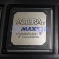
$5000Altera EP3C10E144I7
EP3C10E144I7 FPGA operating at 65nm Technology with 10320 cells and 1.2V voltage


Marken: Altera Corporation (Intel)
Herstellerteil #: EP3C10E144I7
Datenblatt: EP3C10E144I7 Datasheet (PDF)
Paket/Gehäuse: QFP144
Produktart: FPGAs (Field Programmable Gate Array)
RoHS-Status:
Lagerzustand: 2.309 Stück, Neues Original
Warranty: 1 Year Ovaga Warranty - Find Out More
0
1
EP3C10E144I7 Allgemeine Beschreibung
The EP3C10E144I7 is a powerful FPGA developed by Intel, offering a wide range of features including 10,320 logic elements, 366 Kbits of embedded memory, and 288 multipliers. Its low power consumption and high-performance capabilities make it suitable for various applications such as industrial control systems, automotive electronics, and communications equipment. With a maximum operating frequency of 260 MHz and 144 I/O pins, it provides efficient connectivity to external devices. Additionally, its compact size and low power consumption make it ideal for portable and battery-operated devices
Funktionen
- "EP3C" refers to the Cyclone III series of FPGAs, which are programmable logic devices designed for digital logic applications.
- "10" refers to the specific family member within the Cyclone III series, with different numbers indicating different levels of capacity and performance.
- "E144" refers to the package type and pin count. "E144" indicates a 144-pin FineLine BGA (Ball Grid Array) package, which is a type of integrated circuit package with solder balls on the bottom for surface mounting onto a printed circuit board.
- "I7" refers to the speed grade or performance rating of the FPGA. "I7" indicates a commercial-grade (0 to 85 degrees Celsius) device.
Anwendung
- Logic capacity: It has a capacity of up to 10,000 logic elements (LEs), which are the basic building blocks of programmable logic.
- Embedded memory: It may include up to 414 kilobits (Kb) of embedded memory for storing data within the FPGA.
- Digital signal processing (DSP) blocks: It may include up to 54 embedded DSP blocks for implementing high-performance digital signal processing functions.
- I/O interfaces: It may have various I/O interfaces such as GPIO (General Purpose Input/Output) pins, LVDS (Low Voltage Differential Signaling) channels, and other interfaces for communication with external devices.
- Clocking resources: It may include phase-locked loops (PLLs) and clock multiplexers for generating and distributing clock signals within the FPGA.
 Inventory")
Spezifikationen
| Parameter | Wert | Parameter | Wert |
|---|---|---|---|
| feature-family-name | Cyclone® III | feature-process-technology | 65nm |
| feature-maximum-number-of-user-i-os | 94 | feature-number-of-registers | |
| feature-device-logic-cells | 10320 | feature-device-system-gates | |
| feature-number-of-multipliers | 23 (18x18) | feature-program-memory-type | SRAM |
| feature-ram-bits-kbit | 414 | feature-total-number-of-block-ram | 46 |
| feature-ethernet-macs | feature-supported-ip-core | Viterbi Compiler, Low-Speed/Hybrid Serial Decoder|V1 ColdFire|SpeedView Enabled JPEG Encoder (SVE-JPEG-E)|10 Gigabit Ethernet MAC|32/64-bit PCI-X bus Master/Target interface Core, 66/100/133Mhz | |
| feature-supported-ip-core-manufacture | Altera/Freescale/CAST, Inc/MorethanIP/PLDA | feature-maximum-number-of-serdes-channels | |
| feature-device-logic-units | 10320 | feature-device-number-of-dlls-plls | 2 |
| feature-transceiver-blocks | feature-transceiver-speed-gbps | ||
| feature-dedicated-dsp | feature-pci-blocks | ||
| feature-programmability | No | feature-maximum-internal-frequency-mhz | 437.5 |
| feature-speed-grade | 7 | feature-giga-multiply-accumulates-per-second | |
| feature-differential-i-o-standards-supported | LVPECL|LVDS|HSTL-18|HSTL-15|HSTL-12|SSTL-2|SSTL-18|RSDS | feature-single-ended-i-o-standards-supported | LVTTL|LVCMOS|PCI|PCI-X|SSTL|HSTL |
| feature-external-memory-interface | DDR2 SDRAM|QDRII+SRAM | feature-minimum-operating-supply-voltage-v | 1.15 |
| feature-maximum-operating-supply-voltage-v | 1.25 | feature-packaging | |
| feature-rohs | feature-rad-hard | ||
| feature-pin-count | 144 | feature-supplier-package | EQFP EP |
| feature-standard-package-name1 | QFP | feature-cecc-qualified | No |
| feature-esd-protection | feature-escc-qualified | ||
| feature-military | No | feature-aec-qualified | No |
| feature-aec-qualified-number | feature-auto-motive | No | |
| feature-p-pap | No | feature-eccn-code | EAR99 |
| feature-svhc | Yes |
Versand
| Versandart | Versandgebühr | Vorlaufzeit | |
|---|---|---|---|
 |
DHL | $20.00-$40.00 (0.50 KG) | 2-5 Tage |
 |
FedEx | $20.00-$40.00 (0.50 KG) | 2-5 Tage |
 |
UPS | $20.00-$40.00 (0.50 KG) | 2-5 Tage |
 |
TNT | $20.00-$40.00 (0.50 KG) | 2-5 Tage |
 |
EMS | $20.00-$40.00 (0.50 KG) | 2-5 Tage |
 |
REGISTRIERTE LUFTPOST | $20.00-$40.00 (0.50 KG) | 2-5 Tage |
Bearbeitungszeit: Die Versandkosten hängen von der jeweiligen Zone und dem Land ab.
Zahlung
| Zahlungsbedingungen | Handgebühr | |
|---|---|---|
 |
Banküberweisung | Bankgebühr in Höhe von 30,00 USD wird berechnet. |
 |
Paypal | 4,0 % Servicegebühr wird berechnet. |
 |
Kreditkarte | 3,5 % Servicegebühr wird berechnet. |
 |
Western Union | charge US.00 banking fee. |
 |
Geldgramm | Bankgebühr in Höhe von 0,00 USD wird berechnet. |
Garantien
1. Die von Ihnen gekauften elektronischen Bauteile enthalten eine 365-tägige Garantie. Wir garantieren die Produktqualität.
2. Wenn einige der Artikel, die Sie erhalten haben, nicht von perfekter Qualität sind, würden wir verantwortungsvoll Ihre Rückerstattung oder Ersatz arrangieren. Die Artikel müssen jedoch in ihrem Originalzustand verbleiben.
Verpackung
-

Schritt1 :Produkt
-

Schritt2 :Vakuumverpackung
-

Schritt3 :Antistatikbeutel
-

Schritt4 :Individuelle Verpackung
-

Schritt5 :Verpackungskartons
-

Schritt6 :Barcode-Versandetikett


Alle Produkte werden in antistatischen Beuteln verpackt. Versand mit ESD-Antistatikschutz.
Auf dem äußeren ESD-Verpackungsetikett werden die Informationen unseres Unternehmens verwendet: Teilenummer, Marke und Menge.
Wir prüfen alle Waren vor dem Versand, stellen sicher, dass sich alle Produkte in gutem Zustand befinden und dass die Teile neu und original sind und mit dem Datenblatt übereinstimmen.
Nachdem alle Waren darauf überprüft wurden, dass nach dem Verpacken keine Probleme auftreten, werden wir sicher verpacken und per Global Express versenden. Es zeigt eine ausgezeichnete Durchstoß- und Reißfestigkeit sowie eine gute Dichtungsintegrität.


Äquivalente Teile
Für den EP3C10E144I7 Komponente, Sie könnten diese Ersatz- und Alternativteile in Betracht ziehen:
Artikelnummer
Marken
Paket
Beschreibung
Artikelnummer : Embedded
Marken :
Paket :
Beschreibung : systems: It can be used to implement digital logic functions in embedded systems such as industrial automation, robotics, and automotive electronics.
Artikelnummer : Communication
Marken :
Paket :
Beschreibung : systems: It can be used for implementing digital signal processing and communication functions in wireless communication systems, networking equipment, and telecommunications.
Artikelnummer : Test
Marken :
Paket :
Beschreibung : and measurement: It can be used in test and measurement equipment for implementing digital logic functions and signal processing algorithms for data analysis and measurement.
Artikelnummer : Prototyping
Marken :
Paket :
Beschreibung : and validation: It can be used as a prototyping platform for validating and verifying digital logic designs before implementing them in application-specific integrated circuits (ASICs) or other custom hardware.
Teilpunkte
-
The EP3C10E144I7 chip is a member of altera's cyclone iii fpga family. it offers 10,570 logic elements, 308 kilobits of embedded memory, and five phase-locked loops. with integrated high-speed transceivers and low-power consumption, this chip is suitable for a range of applications like digital signal processing, communications, and industrial automation. it supports various i/o standards and provides flexible configuration options, making it a versatile solution for hardware designers.
-
Features
The features of EP3C10E144I7 include a total of 10,320 logic elements, a maximum of 144 user i/o pins, up to 372 kbits of embedded memory, and support for high-speed transceivers. it also offers enhanced low-power capabilities, advanced dsp blocks, high-speed routing, and a flexible i/o structure, making it suitable for a wide range of applications. -
Pinout
The EP3C10E144I7 is a 144-pin fpga (field-programmable gate array) from the cyclone iii family by intel (formerly altera). it has 144 pins and can be used for various functions, such as digital logic control, signal processing, and data management. -
Manufacturer
The manufacturer of the EP3C10E144I7 is altera corporation, which is a semiconductor company specializing in programmable logic devices. -
Application Field
The EP3C10E144I7 is a programmable logic device, so its application areas vary. it can be used in a wide range of industries, including telecommunications, automotive, medical, aerospace, and consumer electronics. it can be used for applications such as signal processing, control systems, image processing, and data storage, among others. -
Package
The EP3C10E144I7 chip is available in a bga package type, with a form factor of 144 pins. the size of the chip is 17x17 mm.


Datenblatt PDF
Wir bieten qualitativ hochwertige Produkte, durchdachten Service und eine Kundendienstgarantie
-

Wir haben reichhaltige Produkte, die Ihre unterschiedlichen Bedürfnisse erfüllen können.
-

Die Mindestbestellmenge beginnt bei 1 Stück.
-

Niedrigste internationale Versandgebühr beginnt ab 0,00 USD
-

365 Tage Qualitätsgarantie für alle Produkte


