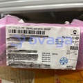
Bilder dienen nur zur Referenz. Siehe Produktspezifikationen.
Bestellungen über
$5000ICE40HX8K-CT256
Programmable circuit device with 960 configurable logic blocks


Marken: Lattice Semiconductor Corporation
Herstellerteil #: ICE40HX8K-CT256
Datenblatt: ICE40HX8K-CT256 Datenblatt (PDF)
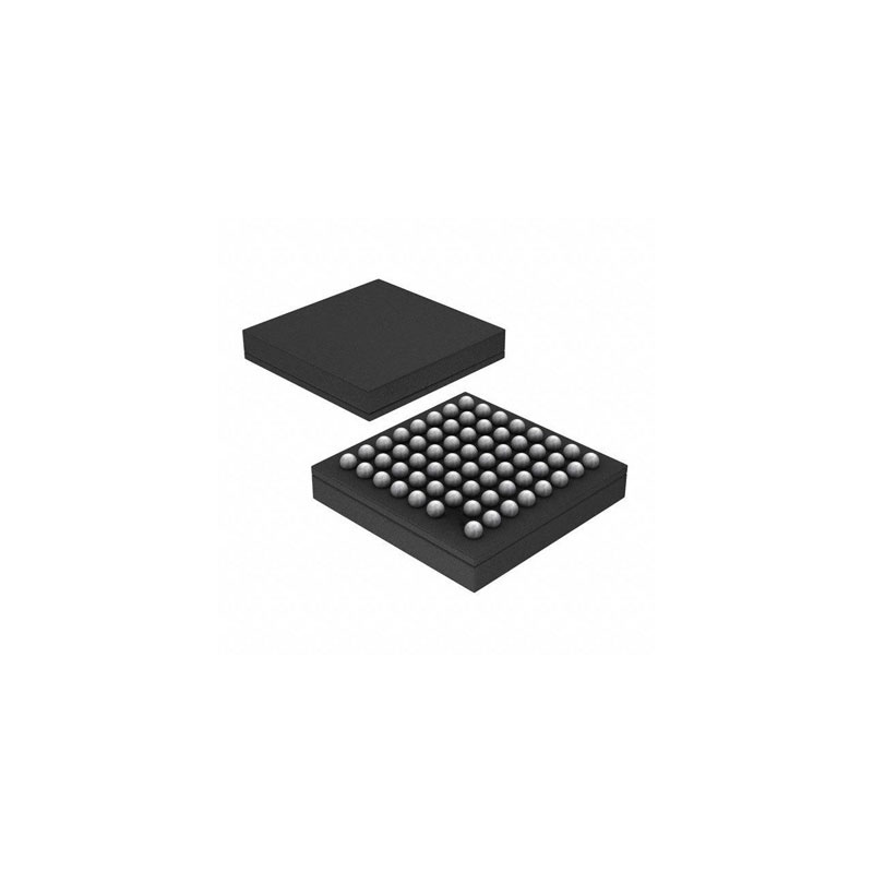
Paket/Gehäuse: 256-LFBGA
Produktart: FPGAs (Field Programmable Gate Array)
RoHS-Status:
Lagerzustand: 7.689 Stück, Neues Original
Warranty: 1 Year Ovaga Warranty - Find Out More
0
1
ICE40HX8K-CT256 Allgemeine Beschreibung
Lattice Semiconductor's ICE40HX8K-CT256 is a standout in the field of low-power FPGAs, offering exceptional performance and features in a compact package. With its 1.2V core voltage and 40nm process technology, this FPGA delivers energy-efficient operation without compromising on power. The device's 8,000 logic cells and 384 Kbits of embedded Block RAM provide ample resources for tackling a variety of digital designs, while the 96 programmable I/O pins ensure seamless connectivity with external devices
Spezifikationen
| Parameter | Wert | Parameter | Wert |
|---|---|---|---|
| Series | iCE40™ HX | Package | Tray |
| Product Status | Active | Programmabe | Not Verified |
| Number of LABs/CLBs | 960 | Number of Logic Elements/Cells | 7680 |
| Total RAM Bits | 131072 | Number of I/O | 206 |
| Voltage - Supply | 1.14V ~ 1.26V | Mounting Type | Surface Mount |
| Operating Temperature | -40°C ~ 100°C (TJ) | Package / Case | 256-LFBGA |
| Supplier Device Package | 256-CABGA (14x14) |
Versand
| Versandart | Versandgebühr | Vorlaufzeit | |
|---|---|---|---|
 |
DHL | $20.00-$40.00 (0.50 KG) | 2-5 Tage |
 |
FedEx | $20.00-$40.00 (0.50 KG) | 2-5 Tage |
 |
UPS | $20.00-$40.00 (0.50 KG) | 2-5 Tage |
 |
TNT | $20.00-$40.00 (0.50 KG) | 2-5 Tage |
 |
EMS | $20.00-$40.00 (0.50 KG) | 2-5 Tage |
 |
REGISTRIERTE LUFTPOST | $20.00-$40.00 (0.50 KG) | 2-5 Tage |
Bearbeitungszeit: Die Versandkosten hängen von der jeweiligen Zone und dem Land ab.
Zahlung
| Zahlungsbedingungen | Handgebühr | |
|---|---|---|
 |
Banküberweisung | Bankgebühr in Höhe von 30,00 USD wird berechnet. |
 |
Paypal | 4,0 % Servicegebühr wird berechnet. |
 |
Kreditkarte | 3,5 % Servicegebühr wird berechnet. |
 |
Western Union | charge US.00 banking fee. |
 |
Geldgramm | Bankgebühr in Höhe von 0,00 USD wird berechnet. |
Garantien
1. Die von Ihnen gekauften elektronischen Bauteile enthalten eine 365-tägige Garantie. Wir garantieren die Produktqualität.
2. Wenn einige der Artikel, die Sie erhalten haben, nicht von perfekter Qualität sind, würden wir verantwortungsvoll Ihre Rückerstattung oder Ersatz arrangieren. Die Artikel müssen jedoch in ihrem Originalzustand verbleiben.
Verpackung
-

Schritt1 :Produkt
-

Schritt2 :Vakuumverpackung
-

Schritt3 :Antistatikbeutel
-

Schritt4 :Individuelle Verpackung
-

Schritt5 :Verpackungskartons
-

Schritt6 :Barcode-Versandetikett


Alle Produkte werden in antistatischen Beuteln verpackt. Versand mit ESD-Antistatikschutz.
Auf dem äußeren ESD-Verpackungsetikett werden die Informationen unseres Unternehmens verwendet: Teilenummer, Marke und Menge.
Wir prüfen alle Waren vor dem Versand, stellen sicher, dass sich alle Produkte in gutem Zustand befinden und dass die Teile neu und original sind und mit dem Datenblatt übereinstimmen.
Nachdem alle Waren darauf überprüft wurden, dass nach dem Verpacken keine Probleme auftreten, werden wir sicher verpacken und per Global Express versenden. Es zeigt eine ausgezeichnete Durchstoß- und Reißfestigkeit sowie eine gute Dichtungsintegrität.


Teilpunkte
-
The ICE40HX8K-CT256 is a low-power FPGA chip from Lattice Semiconductor. It features 7680 logic cells, 3840 LUTs, 120 Kbits of RAM, and 64 I/O pins. With a compact size and low power consumption, this chip is ideal for a wide range of applications in consumer electronics, industrial automation, and IoT devices.
-
Equivalent
Some equivalent products of ICE40HX8K-CT256 chip are ICE40HX1K-CT256, ICE40HX4K-CT256, and ICE40HX16K-CT256. These are other variants of the ICE40HX family of FPGAs that offer different levels of logic capacity and I/O options while maintaining compatibility with the ICE40HX8K-CT256. -
Features
ICE40HX8K-CT256 is a FPGA with 7,680 logic cells, 128 Kbits of embedded block RAM, 20 24-bit math block, and 1 Mbits of embedded non-volatile configuration memory. It has four I/O banks and supports up to 107 user I/Os. It operates on a 1.2V core voltage and 3.3V auxiliary voltage. -
Pinout
The ICE40HX8K-CT256 is a 256-pin FPGS that offers 7680 logic cells and 8 Kb embedded block RAM. It is designed for high-performance applications and has low power consumption. The pin count and functions include I/O, clock input/output, configuration, and power supply connections. -
Manufacturer
The ICE40HX8K-CT256 is manufactured by Lattice Semiconductor Corporation. Lattice Semiconductor is a semiconductor company that designs and manufactures programmable logic devices, software development tools, and IP (intellectual property) cores. They specialize in creating low-power, small form factor products for the consumer, communications, industrial, automotive, and other markets. -
Application Field
The ICE40HX8K-CT256 is commonly used in applications such as mobile devices, IoT (Internet of Things) devices, sensor interfaces, battery management systems, and low-power applications. Its small form factor, low power consumption, and integrated features make it well-suited for embedded applications that require compact and energy-efficient designs. -
Package
The ICE40HX8K-CT256 chip is available in a CT256 package type, with a form of BGA (Ball Grid Array), and a size of 17mm x 17mm.
Wir bieten qualitativ hochwertige Produkte, durchdachten Service und eine Kundendienstgarantie
-

Wir haben reichhaltige Produkte, die Ihre unterschiedlichen Bedürfnisse erfüllen können.
-

Die Mindestbestellmenge beginnt bei 1 Stück.
-

Niedrigste internationale Versandgebühr beginnt ab 0,00 USD
-

365 Tage Qualitätsgarantie für alle Produkte