Bilder dienen nur zur Referenz. Siehe Produktspezifikationen.
Bestellungen über
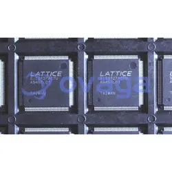
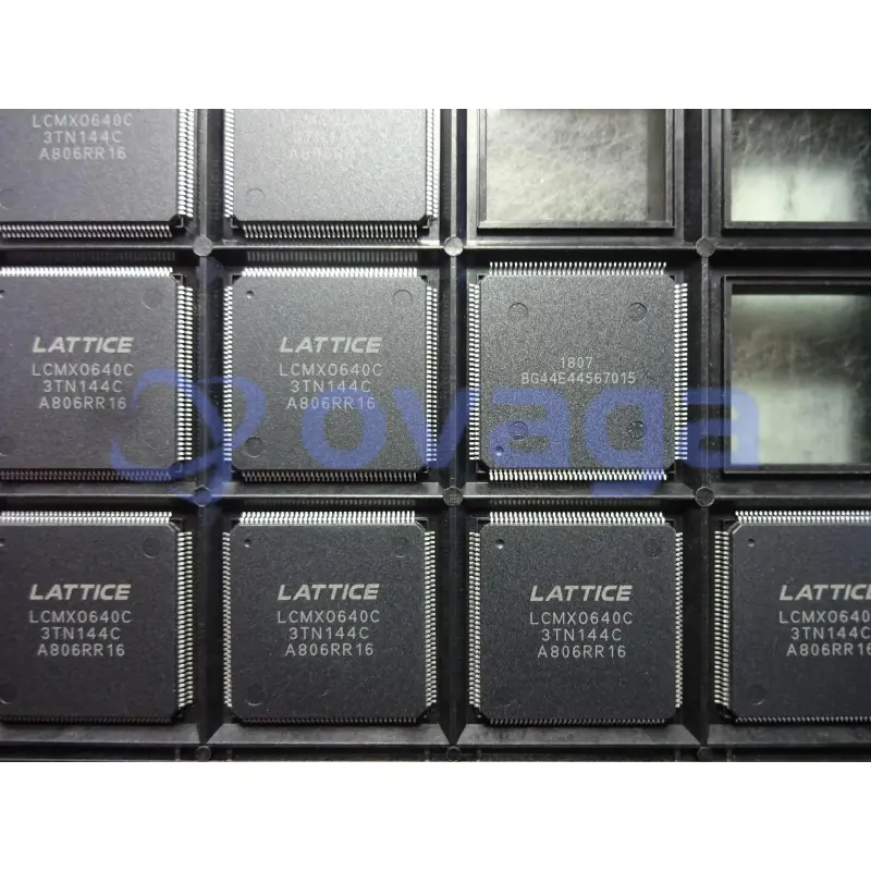
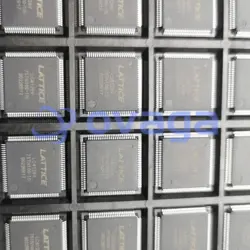
$5000LATTICE LCMXO640C-3TN144C
Programmable FPGA with 640 LUTs and 113 I/O


Marken: LATTICE
Herstellerteil #: LCMXO640C-3TN144C
Datenblatt: LCMXO640C-3TN144C Datenblatt (PDF)
Paket/Gehäuse: TQFP144
Produktart: FPGAs (Field Programmable Gate Array)
RoHS-Status:
Lagerzustand: 9.458 Stück, Neues Original
Warranty: 1 Year Ovaga Warranty - Find Out More
0
1
LCMXO640C-3TN144C Allgemeine Beschreibung
When it comes to programmability and flexibility, the LCMXO640C-3TN144C FPGA stands out with its field programmable gate array technology. This FPGA offers engineers the ability to customize their logic functions according to specific application requirements. With the 640 LUTs onboard, designers have ample resources to implement complex algorithms and logic operations efficiently
Funktionen
- Non-volatile, Infinitely Reconfigurable
- Instant-on – powers up in microseconds
- Single chip, no external configuration memory
- required
- Excellent design security, no bit stream to
- intercept
- Reconfigure SRAM based logic in milliseconds
- SRAM and non-volatile memory programmable
- through JTAG port
- Supports background programming of
- non-volatile memory
- Sleep Mode
- Allows up to 100x static current reduction
- TransFR™ Reconfiguration (TFR)
- In-field logic update while system operates
- High I/O to Logic Density
- 256 to 2280 LUT4s
- 73 to 271 I/Os with extensive package options
- Density migration supported
- Lead free/RoHS compliant packaging
- Embedded and Distributed Memory
- Up to 27.6 Kbits sysMEM™ Embedded Block
- RAM
- Up to 7.5 Kbits distributed RAM
- Dedicated FIFO control logic
- Flexible I/O Buffer
- Programmable sysIO™ buffer supports wide
- range of interfaces:
- − LVCMOS 3.3/2.5/1.8/1.5/1.2
- − LVTTL
- − PCI
- − LVDS, Bus-LVDS, LVPECL, RSDS
- sysCLOCK™ PLLs
- Up to two analog PLLs per device
- Clock multiply, divide, and phase shifting
- System Level Support
- IEEE Standard 1149.1 Boundary Scan
- Onboard oscillator
- Devices operate with 3.3V, 2.5V, 1.8V or 1.2V
- power supply
- IEEE 1532 compliant in-system programming

Spezifikationen
| Parameter | Wert | Parameter | Wert |
|---|---|---|---|
| Product Category | FPGA - Field Programmable Gate Array | RoHS | Details |
| Series | LCMXO640C | Number of Logic Elements | 640 LE |
| Adaptive Logic Modules - ALMs | 320 ALM | Embedded Memory | 0 bit |
| Number of I/Os | 113 I/O | Supply Voltage - Min | 1.71 V |
| Supply Voltage - Max | 3.465 V | Minimum Operating Temperature | 0 C |
| Maximum Operating Temperature | + 85 C | Mounting Style | SMD/SMT |
| Package / Case | CSBGA-144 | Brand | Lattice |
| Distributed RAM | 6.1 kbit | Height | 1.4 mm |
| Length | 20 mm | Maximum Operating Frequency | 500 MHz |
| Moisture Sensitive | Yes | Number of Logic Array Blocks - LABs | 80 LAB |
| Operating Supply Current | 17 mA | Operating Supply Voltage | 1.8 V/2.5 V/3.3 V |
| Product Type | FPGA - Field Programmable Gate Array | Factory Pack Quantity | 60 |
| Subcategory | Programmable Logic ICs | Total Memory | 6.1 kbit |
| Width | 20 mm |
Versand
| Versandart | Versandgebühr | Vorlaufzeit | |
|---|---|---|---|
 |
DHL | $20.00-$40.00 (0.50 KG) | 2-5 Tage |
 |
FedEx | $20.00-$40.00 (0.50 KG) | 2-5 Tage |
 |
UPS | $20.00-$40.00 (0.50 KG) | 2-5 Tage |
 |
TNT | $20.00-$40.00 (0.50 KG) | 2-5 Tage |
 |
EMS | $20.00-$40.00 (0.50 KG) | 2-5 Tage |
 |
REGISTRIERTE LUFTPOST | $20.00-$40.00 (0.50 KG) | 2-5 Tage |
Bearbeitungszeit: Die Versandkosten hängen von der jeweiligen Zone und dem Land ab.
Zahlung
| Zahlungsbedingungen | Handgebühr | |
|---|---|---|
 |
Banküberweisung | Bankgebühr in Höhe von 30,00 USD wird berechnet. |
 |
Paypal | 4,0 % Servicegebühr wird berechnet. |
 |
Kreditkarte | 3,5 % Servicegebühr wird berechnet. |
 |
Western Union | charge US.00 banking fee. |
 |
Geldgramm | Bankgebühr in Höhe von 0,00 USD wird berechnet. |
Garantien
1. Die von Ihnen gekauften elektronischen Bauteile enthalten eine 365-tägige Garantie. Wir garantieren die Produktqualität.
2. Wenn einige der Artikel, die Sie erhalten haben, nicht von perfekter Qualität sind, würden wir verantwortungsvoll Ihre Rückerstattung oder Ersatz arrangieren. Die Artikel müssen jedoch in ihrem Originalzustand verbleiben.
Verpackung
-

Schritt1 :Produkt
-

Schritt2 :Vakuumverpackung
-

Schritt3 :Antistatikbeutel
-

Schritt4 :Individuelle Verpackung
-

Schritt5 :Verpackungskartons
-

Schritt6 :Barcode-Versandetikett


Alle Produkte werden in antistatischen Beuteln verpackt. Versand mit ESD-Antistatikschutz.
Auf dem äußeren ESD-Verpackungsetikett werden die Informationen unseres Unternehmens verwendet: Teilenummer, Marke und Menge.
Wir prüfen alle Waren vor dem Versand, stellen sicher, dass sich alle Produkte in gutem Zustand befinden und dass die Teile neu und original sind und mit dem Datenblatt übereinstimmen.
Nachdem alle Waren darauf überprüft wurden, dass nach dem Verpacken keine Probleme auftreten, werden wir sicher verpacken und per Global Express versenden. Es zeigt eine ausgezeichnete Durchstoß- und Reißfestigkeit sowie eine gute Dichtungsintegrität.


Teilpunkte
-
The LCMXO640C-3TN144C is a programmable logic device (PLD) chip manufactured by Lattice Semiconductor. It belongs to the Lattice XO2 family of FPGAs and has 640 Look-Up Tables (LUTs) and 640 logical registers. With a density of 640 LUTs, this chip offers a cost-effective and low-power solution for a variety of applications such as consumer electronics, industrial automation, and communication devices.
-
Features
LCMXO640C-3TN144C is a low-power, non-volatile PLD (Programmable Logic Device) with a capacity of 640 Look-Up Tables (LUTs) and 32640 bits of RAM. It operates with a supply voltage of 3.3V and offers 144-pin TQFP packaging. Additionally, it features an internal oscillator and programmable routing to cater to various digital designs. -
Pinout
The LCMXO640C-3TN144C is a Field-Programmable Gate Array (FPGA) with a pin count of 144. It functions as a programmable logic device that can be configured to perform various digital functions. -
Manufacturer
The manufacturer of the LCMXO640C-3TN144C is Lattice Semiconductor Corporation. It is a semiconductor company that specializes in the design and manufacture of programmable logic devices, including field-programmable gate arrays (FPGAs) and complex programmable logic devices (CPLDs). -
Application Field
The LCMXO640C-3TN144C can be used in various application areas such as portable consumer electronics, industrial automation, automotive systems, and communication devices. -
Package
The LCMXO640C-3TN144C chip has a package type of TQFP (Thin Quad Flat Package), a form of leaded surface mount, and a size of 14 x 14 mm.


Wir bieten qualitativ hochwertige Produkte, durchdachten Service und eine Kundendienstgarantie
-

Wir haben reichhaltige Produkte, die Ihre unterschiedlichen Bedürfnisse erfüllen können.
-

Die Mindestbestellmenge beginnt bei 1 Stück.
-

Niedrigste internationale Versandgebühr beginnt ab 0,00 USD
-

365 Tage Qualitätsgarantie für alle Produkte