Bilder dienen nur zur Referenz. Siehe Produktspezifikationen.
Bestellungen über
$5000MXIC MX25L512MC-12G
High-capacity, low-voltage NOR Flash chip for efficient data storage and retrieval


Marken: MXIC
Herstellerteil #: MX25L512MC-12G
Datenblatt: MX25L512MC-12G Datenblatt (PDF)
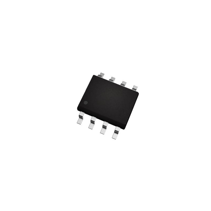
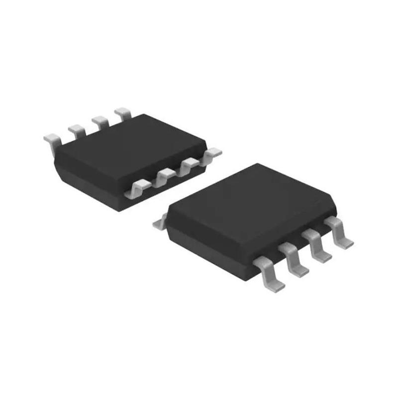
Paket/Gehäuse: SOP-8
Produktart: Microcontrollers
RoHS-Status:
Lagerzustand: 5.290 Stück, Neues Original
Warranty: 1 Year Ovaga Warranty - Find Out More
0
1
MX25L512MC-12G Allgemeine Beschreibung
GENERAL DESCRIPTION MX25L1005 is a CMOS 1,048,576 bit serial Flash memory, which is configured as 131,072 x 8 internally.The MX25L1005 feature a serial peripheral interface and software protocol allowing operation on a simple 3-wire bus. The three bus signals are a clock input (SCLK), a serial data input (SI), and a serial data output (SO). SPI access to the device is enabled by CS# input. The MX25L1005 provide sequential read operation on whole chip. After program/erase command is issued, auto program/ erase algorithms which program/ erase and verify the specified page or sector/block locations will be executed. Program command is executed on page (256 bytes) basis, and erase command is executes on chip or sector(4K-bytes) or block(64K-bytes). To provide user with ease of interface, a status register is included to indicate the status of the chip. The status read command can be issued to detect completion status of a program or erase operation via WIP bit. When the device is not in operation and CS# is high, it is put in standby mode and draws less than 10uA DC current. The MX25L1005 utilize MXIC's proprietary memory cell, which reliably stores memory contents even after 100,000 program and erase cycles.FEATURES GENERAL • Serial Peripheral Interface (SPI) compatible -- Mode 0 and Mode 3 • 1,048,576 x 1 bit structure • 32 Equal Sectors with 4K byte each - Any Sector can be erased individually • 2 Equal Blocks with 64K byte each - Any Block can be erased individually • Single Power Supply Operation - 2.7 to 3.6 volt for read, erase, and program operations • Latch-up protected to 100mA from -1V to Vcc +1V • Low Vcc write inhibit is from 1.5V to 2.5VPERFORMANCE • High Performance - Fast access time: 85MHz serial clock (15pF + 1TTL Load) and 66MHz serial clock (30pF + 1TTL Load) - Fast program time: 1.4ms(typ.) and 5ms(max.)/page (256-byte per page) - Fast erase time: 60ms(typ.) and 120ms(max.)/sector (4K-byte per sector) ; 1s(typ.) and 2s(max.)/block (64K-byte per block) • Low Power Consumption - Low active read current: 12mA(max.) at 85MHz, 8mA(max.) at 66MHz and 4mA(max.) at 33MHz - Low active programming current: 15mA (max.) - Low active erase current: 15mA (max.) - Low standby current: 10uA (max.) - Deep power-down mode 1uA (typical) • Minimum 100,000 erase/program cyclesSOFTWARE FEATURES • Input Data Format - 1-byte Command code • Block Lock protection - The BP0~BP1 status bit defines the size of the area to be software protected against Program and Erase instructions. • Auto Erase and Auto Program Algorithm - Automatically erases and verifies data at selected sector - Automatically programs and verifies data at selected page by an internal algorithm that automatically times the program pulse widths (Any page to be programed should have page in the erased state first) • Status Register Feature • Electronic Identification - JEDEC 2-byte Device ID - RES command, 1-byte Device IDHARDWARE FEATURES • SCLK Input - Serial clock input • SI Input - Serial Data Input • SO Output - Serial Data Output • WP# pin - Hardware write protection • HOLD# pin - pause the chip without diselecting the chip • PACKAGE - 8-pin SOP (150mil) - 8-land USON (2x3x0.6mm)* - All Pb-free devices are RoHS Compliant
Funktionen
- GENERAL
- Serial Peripheral Interface (SPI) compatible -- Mode 0 and Mode 3
- 1,048,576 x 1 bit structure
- 32 Equal Sectors with 4K byte each
- - Any Sector can be erased individually
- 2 Equal Blocks with 64K byte each
- - Any Block can be erased individually
- Single Power Supply Operation
- - 2.7 to 3.6 volt for read, erase, and program operations
- Latch-up protected to 100mA from -1V to Vcc +1V
- Low Vcc write inhibit is from 1.5V to 2.5V
- PERFORMANCE
- High Performance
- - Fast access time: 85MHz serial clock (15pF + 1TTL Load) and 66MHz serial clock (30pF + 1TTL Load)
- - Fast program time: 1.4ms(typ.) and 5ms(max.)/page (256-byte per page)
- - Fast erase time: 60ms(typ.) and 120ms(max.)/sector (4K-byte per sector) ; 1s(typ.) and 2s(max.)/block (64K-byte per block)
- Low Power Consumption
- - Low active read current: 12mA(max.) at 85MHz, 8mA(max.) at 66MHz and 4mA(max.) at 33MHz
- - Low active programming current: 15mA (max.)
- - Low active erase current: 15mA (max.)
- - Low standby current: 10uA (max.)
- - Deep power-down mode 1uA (typical)
- Minimum 100,000 erase/program cycles
- SOFTWARE FEATURES
- Input Data Format
- - 1-byte Command code
- Block Lock protection
- - The BP0~BP1 status bit defines the size of the area to be software protected against Program and Erase instructions.
- Auto Erase and Auto Program Algorithm
- - Automatically erases and verifies data at selected sector
- - Automatically programs and verifies data at selected page by an internal algorithm that automatically times the program pulse widths (Any page to be programed should have page in the erased state first)
- Status Register Feature
- Electronic Identification
- - JEDEC 2-byte Device ID
- - RES command, 1-byte Device ID
- HARDWARE FEATURES
- SCLK Input
- - Serial clock input
- SI Input
- - Serial Data Input
- SO Output
- - Serial Data Output
- WP# pin
- - Hardware write protection
- HOLD# pin
- - pause the chip without diselecting the chip
- PACKAGE
- - 8-pin SOP (150mil)
- - 8-land USON (2x3x0.6mm)
- - All Pb-free devices are RoHS Compliant

Spezifikationen
| Parameter | Wert | Parameter | Wert |
|---|---|---|---|
| Manufacturer | Macronix |
Versand
| Versandart | Versandgebühr | Vorlaufzeit | |
|---|---|---|---|
 |
DHL | $20.00-$40.00 (0.50 KG) | 2-5 Tage |
 |
FedEx | $20.00-$40.00 (0.50 KG) | 2-5 Tage |
 |
UPS | $20.00-$40.00 (0.50 KG) | 2-5 Tage |
 |
TNT | $20.00-$40.00 (0.50 KG) | 2-5 Tage |
 |
EMS | $20.00-$40.00 (0.50 KG) | 2-5 Tage |
 |
REGISTRIERTE LUFTPOST | $20.00-$40.00 (0.50 KG) | 2-5 Tage |
Bearbeitungszeit: Die Versandkosten hängen von der jeweiligen Zone und dem Land ab.
Zahlung
| Zahlungsbedingungen | Handgebühr | |
|---|---|---|
 |
Banküberweisung | Bankgebühr in Höhe von 30,00 USD wird berechnet. |
 |
Paypal | 4,0 % Servicegebühr wird berechnet. |
 |
Kreditkarte | 3,5 % Servicegebühr wird berechnet. |
 |
Western Union | charge US.00 banking fee. |
 |
Geldgramm | Bankgebühr in Höhe von 0,00 USD wird berechnet. |
Garantien
1. Die von Ihnen gekauften elektronischen Bauteile enthalten eine 365-tägige Garantie. Wir garantieren die Produktqualität.
2. Wenn einige der Artikel, die Sie erhalten haben, nicht von perfekter Qualität sind, würden wir verantwortungsvoll Ihre Rückerstattung oder Ersatz arrangieren. Die Artikel müssen jedoch in ihrem Originalzustand verbleiben.
Verpackung
-

Schritt1 :Produkt
-

Schritt2 :Vakuumverpackung
-

Schritt3 :Antistatikbeutel
-

Schritt4 :Individuelle Verpackung
-

Schritt5 :Verpackungskartons
-

Schritt6 :Barcode-Versandetikett


Alle Produkte werden in antistatischen Beuteln verpackt. Versand mit ESD-Antistatikschutz.
Auf dem äußeren ESD-Verpackungsetikett werden die Informationen unseres Unternehmens verwendet: Teilenummer, Marke und Menge.
Wir prüfen alle Waren vor dem Versand, stellen sicher, dass sich alle Produkte in gutem Zustand befinden und dass die Teile neu und original sind und mit dem Datenblatt übereinstimmen.
Nachdem alle Waren darauf überprüft wurden, dass nach dem Verpacken keine Probleme auftreten, werden wir sicher verpacken und per Global Express versenden. Es zeigt eine ausgezeichnete Durchstoß- und Reißfestigkeit sowie eine gute Dichtungsintegrität.


Wir bieten qualitativ hochwertige Produkte, durchdachten Service und eine Kundendienstgarantie
-

Wir haben reichhaltige Produkte, die Ihre unterschiedlichen Bedürfnisse erfüllen können.
-

Die Mindestbestellmenge beginnt bei 1 Stück.
-

Niedrigste internationale Versandgebühr beginnt ab 0,00 USD
-

365 Tage Qualitätsgarantie für alle Produkte


Empfehlen
-
![MX25L6445EM2I]()
MXIC
-
![MX25L512MC]()
MXIC
-
![MX25L1005AMC]()
MXIC
-
![MX25-10G]()
MXIC