

Bilder dienen nur zur Referenz. Siehe Produktspezifikationen.
Bestellungen über
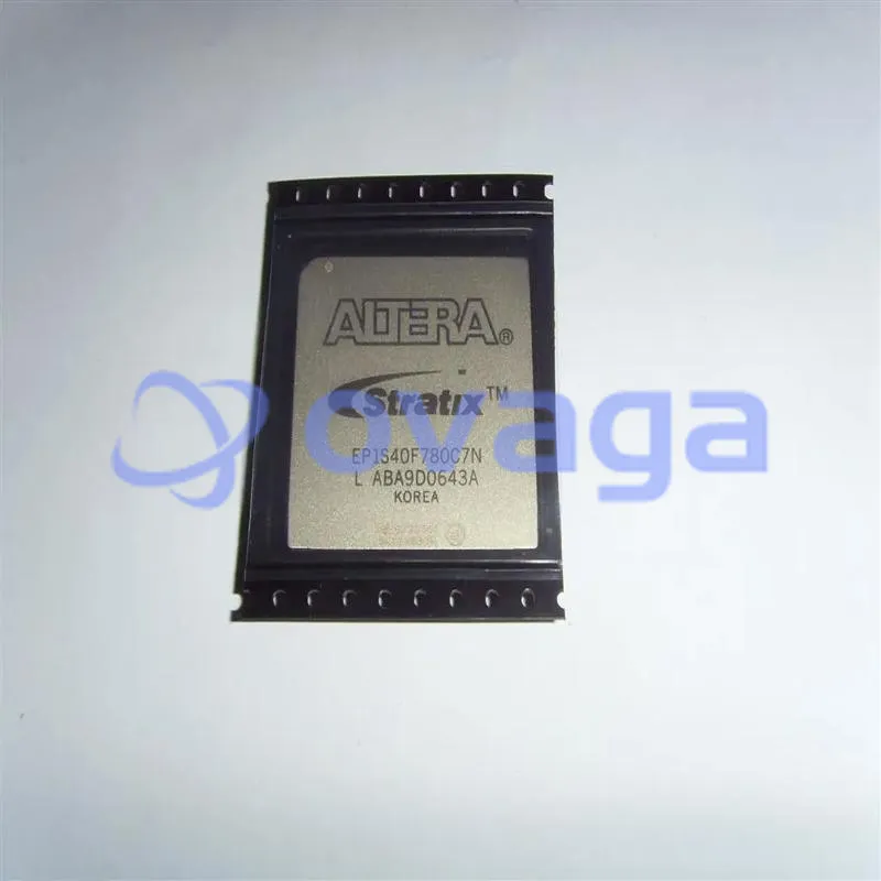
$5000Intel EP1S40F780C7N
Sample Product Description for Developmental Purposes


Marken: Intel
Herstellerteil #: EP1S40F780C7N
Datenblatt: EP1S40F780C7N Datenblatt (PDF)
Paket/Gehäuse: FBGA-780
Produktart: FPGAs (Field Programmable Gate Array)
RoHS-Status:
Lagerzustand: 6.554 Stück, Neues Original
Warranty: 1 Year Ovaga Warranty - Find Out More
0
1
EP1S40F780C7N Allgemeine Beschreibung
Altera's EP1S40F780C7N FPGA is a technological marvel, featuring 40,000 logic elements and 780Kbits of embedded memory powered by a 90nm processing technology. With 7,680 logic array blocks and 280 embedded multipliers, this FPGA is designed to excel in high-performance applications requiring complex logic functions, signal processing, and connectivity capabilities. Operating at a maximum internal frequency of 260MHz, the EP1S40F780C7N ensures swift execution of operations, while supporting communication protocols like PCI Express, Gigabit Ethernet, and SATA for seamless connectivity. Whether it's handling intricate algorithms or processing large volumes of data, this FPGA delivers unmatched performance and reliability
Funktionen
Configuration devices for SRAM-based LUT devices offer the following features:
Configures Altera ACEX 1K, APEX 20K (including APEX 20K, APEX 20KC, and APEX 20KE), APEX II, Arria GX, Cyclone, Cyclone II, FLEX 10K (including FLEX 10KE and FLEX 10KA) Mercury, Stratix, Stratix GX, Stratix II, and Stratix II GX devices
Easy-to-use four-pin interface
Low current during configuration and near-zero standby mode current
Programming support with the Altera Programming Unit (APU) and programming hardware from Data I/O, BP Microsystems, and other third-party programmers
Available in compact plastic packages
8-pin plastic dual in-line (PDIP) package
20-pin plastic J-lead chip carrier (PLCC) package
32-pin plastic thin quad flat pack (TQFP) package
EPC2 device has reprogrammable flash configuration memory
5.0-V and 3.3-V in-system programmability (ISP) through the built-in IEEE Std.
1149.1 JTAG interface
Built-in JTAG boundary-scan test (BST) circuitry compliant with IEEE Std. 1149.1
Supports programming through Serial Vector Format File (.svf), Jam Standard Test and Programming Language (STAPL) Format File (.jam), JAM Byte Code File (.jbc), and the Quartus II and MAX+PLUS II softwares using the USB-Blaster, MasterBlaster, ByteBlaster II, EthernetBlaster, or ByteBlasterMV download cable
Supports programming through Programmer Object File (.pof) for EPC1 and EPC1441 devices
nINIT_CONF pin allows INIT_CONF JTAG instruction to begin FPGA configuration

Spezifikationen
| Parameter | Wert | Parameter | Wert |
|---|---|---|---|
| Manufacturer | Intel | Product Category | FPGA - Field Programmable Gate Array |
| Shipping Restrictions | This product may require additional documentation to export from the United States. | RoHS | Details |
| Series | Stratix EP1S40 | Number of Logic Elements | 41250 LE |
| Adaptive Logic Modules - ALMs | - | Embedded Memory | 3.27 Mbit |
| Number of I/Os | 615 I/O | Supply Voltage - Min | 1.5 V |
| Supply Voltage - Max | 1.5 V | Minimum Operating Temperature | 0 C |
| Maximum Operating Temperature | + 70 C | Mounting Style | SMD/SMT |
| Package / Case | FBGA-780 | Packaging | ["Tray"] |
| Brand | Intel / Altera | Maximum Operating Frequency | 66 MHz |
| Moisture Sensitive | Yes | Number of Logic Array Blocks - LABs | 4125 LAB |
| Operating Supply Current | 145 mA | Operating Supply Voltage | 1.5 V |
| Product Type | FPGA - Field Programmable Gate Array | Factory Pack Quantity | 36 |
| Subcategory | Programmable Logic ICs | Total Memory | 3423744 bit |
| Tradename | Stratix |
Versand
| Versandart | Versandgebühr | Vorlaufzeit | |
|---|---|---|---|
 |
DHL | $20.00-$40.00 (0.50 KG) | 2-5 Tage |
 |
FedEx | $20.00-$40.00 (0.50 KG) | 2-5 Tage |
 |
UPS | $20.00-$40.00 (0.50 KG) | 2-5 Tage |
 |
TNT | $20.00-$40.00 (0.50 KG) | 2-5 Tage |
 |
EMS | $20.00-$40.00 (0.50 KG) | 2-5 Tage |
 |
REGISTRIERTE LUFTPOST | $20.00-$40.00 (0.50 KG) | 2-5 Tage |
Bearbeitungszeit: Die Versandkosten hängen von der jeweiligen Zone und dem Land ab.
Zahlung
| Zahlungsbedingungen | Handgebühr | |
|---|---|---|
 |
Banküberweisung | Bankgebühr in Höhe von 30,00 USD wird berechnet. |
 |
Paypal | 4,0 % Servicegebühr wird berechnet. |
 |
Kreditkarte | 3,5 % Servicegebühr wird berechnet. |
 |
Western Union | charge US.00 banking fee. |
 |
Geldgramm | Bankgebühr in Höhe von 0,00 USD wird berechnet. |
Garantien
1. Die von Ihnen gekauften elektronischen Bauteile enthalten eine 365-tägige Garantie. Wir garantieren die Produktqualität.
2. Wenn einige der Artikel, die Sie erhalten haben, nicht von perfekter Qualität sind, würden wir verantwortungsvoll Ihre Rückerstattung oder Ersatz arrangieren. Die Artikel müssen jedoch in ihrem Originalzustand verbleiben.
Verpackung
-

Schritt1 :Produkt
-

Schritt2 :Vakuumverpackung
-

Schritt3 :Antistatikbeutel
-

Schritt4 :Individuelle Verpackung
-

Schritt5 :Verpackungskartons
-

Schritt6 :Barcode-Versandetikett


Alle Produkte werden in antistatischen Beuteln verpackt. Versand mit ESD-Antistatikschutz.
Auf dem äußeren ESD-Verpackungsetikett werden die Informationen unseres Unternehmens verwendet: Teilenummer, Marke und Menge.
Wir prüfen alle Waren vor dem Versand, stellen sicher, dass sich alle Produkte in gutem Zustand befinden und dass die Teile neu und original sind und mit dem Datenblatt übereinstimmen.
Nachdem alle Waren darauf überprüft wurden, dass nach dem Verpacken keine Probleme auftreten, werden wir sicher verpacken und per Global Express versenden. Es zeigt eine ausgezeichnete Durchstoß- und Reißfestigkeit sowie eine gute Dichtungsintegrität.


Teilpunkte
-
The EP1S40F780C7N chip is a high-performance field-programmable gate array (FPGA) developed by Altera (now part of Intel). It features 40,000 logic elements, a maximum of 780 I/O pins, and is suitable for a wide range of applications including communication systems, industrial automation, and consumer electronics.
-
Equivalent
The equivalent products of EP1S40F780C7N chip are Altera Cyclone series chips such as EP1S80F780C7N, EP1C12F324C8N, and EP1C20F324C8N. These chips have similar functionality and are also used for high-performance computing applications. -
Features
EP1S40F780C7N is an Altera Stratix device with 39,264 logic elements, 3.7 Mb embedded memory, and 386 I/O pins. It features LVDS, RSDS, and HSTL I/O standards, up to 780 Kbits of user flash memory, and support for functional safety applications with safety certifications. -
Pinout
The EP1S40F780C7N is a 780-pin Field Programmable Gate Array (FPGA) with 40,000 logic elements. It has various functions such as arithmetic operations, signal processing, and digital communication. It also includes 20 embedded 18-bit multipliers, offering high performance for a wide range of applications. -
Manufacturer
The manufacturer of the EP1S40F780C7N is Intel Corporation. Intel is an American multinational corporation specializing in semiconductor design, development, and manufacturing. They are one of the world's largest and highest-valued semiconductor chip makers based on revenue. Intel produces a wide range of processors and other semiconductor products for a variety of industries including computing, networking, data storage, and communication. -
Application Field
The EP1S40F780C7N is a field-programmable gate array (FPGA) that can be used in a variety of applications such as telecommunications, networking, industrial automation, military and aerospace systems, and image processing. It offers high-speed processing capabilities and flexibility for a wide range of complex digital designs. -
Package
The EP1S40F780C7N chip is a flip-chip BGA (Ball Grid Array) package type with a size of 780-ball and a form factor of 31mm x 31mm.


Wir bieten qualitativ hochwertige Produkte, durchdachten Service und eine Kundendienstgarantie
-

Wir haben reichhaltige Produkte, die Ihre unterschiedlichen Bedürfnisse erfüllen können.
-

Die Mindestbestellmenge beginnt bei 1 Stück.
-

Niedrigste internationale Versandgebühr beginnt ab 0,00 USD
-

365 Tage Qualitätsgarantie für alle Produkte


