

Bilder dienen nur zur Referenz. Siehe Produktspezifikationen.
Bestellungen über
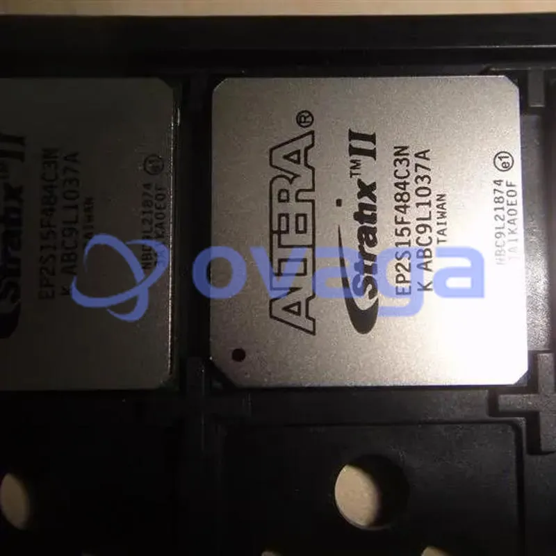
$5000Intel EP2S15F484C3N
FC-FBGA packaged EP2S15F484C3N FPGA, part of the Stratix® II Family with a maximum frequency of 816.99MHz


Marken: Intel
Herstellerteil #: EP2S15F484C3N
Datenblatt: EP2S15F484C3N Datenblatt (PDF)
Paket/Gehäuse: FBGA-484
Produktart: FPGAs (Field Programmable Gate Array)
RoHS-Status:
Lagerzustand: 9.614 Stück, Neues Original
Warranty: 1 Year Ovaga Warranty - Find Out More
0
1
EP2S15F484C3N Allgemeine Beschreibung
The EP2S15F484C3N is a high-performance FPGA Logic IC that belongs to the renowned Stratix II series. Boasting 342 I/Os and advanced clock management features such as PLL and DLL, this IC offers exceptional versatility and functionality. It operates at a 3.3V I/O supply voltage and can withstand temperatures from 0°C to +85°C, making it suitable for diverse operating environments. With a FBGA logic case style and 484 pins, it is designed for secure and efficient integration into various electronic designs. Furthermore, this product is RoHS compliant, reflecting its adherence to strict environmental standards
Funktionen
- 15,600 to 179,400 equivalent LEs New and innovative adaptive logic module (ALM), the basic building block of the Stratix II architecture, maximizes performance and resource usage efficiency Up to 9,383,040 RAM bits (1,172,880 bytes) available without reducing logic resources TriMatrix memory consisting of three RAM block sizes to implement true dual-port memory and first-in first-out (FIFO) buffers High-speed DSP blocks provide dedicated implementation of multipliers (at up to 450 MHz), multiply-accumulate functions, and finite impulse response (FIR) filters Up to 16 global clocks with 24 clocking resources per device region Clock control blocks support dynamic clock network enable/disable, which allows clock networks to power down to reduce power consumption in user mode Up to 12 PLLs (four enhanced PLLs and eight fast PLLs) per device provide spread spectrum, programmable bandwidth, clock switchover, real-time PLL reconfiguration, and advanced multiplication and phase shifting Support for numerous single-ended and differential I/O standards High-speed differential I/O support with DPA circuitry for 1-Gbps performance Support for high-speed networking and communications bus standards including Parallel RapidIO, SPI-4 Phase 2 (POS-PHY Level 4), HyperTransport™ technology, and SFI-4 Support for high-speed external memory, including DDR and DDR2 SDRAM, RLDRAM II, QDR II SRAM, and SDR SDRAM Support for multiple intellectual property megafunctions from Altera MegaCore® functions and Altera Megafunction Partners Program (AMPPSM) megafunctions Support for design security using configuration bitstream encryption Support for remote configuration updates
Spezifikationen
| Parameter | Wert | Parameter | Wert |
|---|---|---|---|
| Product Status | Obsolete | Programmabe | Not Verified |
| Number of LABs/CLBs | 780 | Number of Logic Elements/Cells | 15600 |
| Total RAM Bits | 419328 | Number of I/O | 342 |
| Number of Gates | - | Voltage - Supply | 1.15V ~ 1.25V |
| Mounting Type | Surface Mount | Operating Temperature | 0°C ~ 85°C (TJ) |
| Package / Case | 484-BBGA |
Versand
| Versandart | Versandgebühr | Vorlaufzeit | |
|---|---|---|---|
 |
DHL | $20.00-$40.00 (0.50 KG) | 2-5 Tage |
 |
FedEx | $20.00-$40.00 (0.50 KG) | 2-5 Tage |
 |
UPS | $20.00-$40.00 (0.50 KG) | 2-5 Tage |
 |
TNT | $20.00-$40.00 (0.50 KG) | 2-5 Tage |
 |
EMS | $20.00-$40.00 (0.50 KG) | 2-5 Tage |
 |
REGISTRIERTE LUFTPOST | $20.00-$40.00 (0.50 KG) | 2-5 Tage |
Bearbeitungszeit: Die Versandkosten hängen von der jeweiligen Zone und dem Land ab.
Zahlung
| Zahlungsbedingungen | Handgebühr | |
|---|---|---|
 |
Banküberweisung | Bankgebühr in Höhe von 30,00 USD wird berechnet. |
 |
Paypal | 4,0 % Servicegebühr wird berechnet. |
 |
Kreditkarte | 3,5 % Servicegebühr wird berechnet. |
 |
Western Union | charge US.00 banking fee. |
 |
Geldgramm | Bankgebühr in Höhe von 0,00 USD wird berechnet. |
Garantien
1. Die von Ihnen gekauften elektronischen Bauteile enthalten eine 365-tägige Garantie. Wir garantieren die Produktqualität.
2. Wenn einige der Artikel, die Sie erhalten haben, nicht von perfekter Qualität sind, würden wir verantwortungsvoll Ihre Rückerstattung oder Ersatz arrangieren. Die Artikel müssen jedoch in ihrem Originalzustand verbleiben.
Verpackung
-

Schritt1 :Produkt
-

Schritt2 :Vakuumverpackung
-

Schritt3 :Antistatikbeutel
-

Schritt4 :Individuelle Verpackung
-

Schritt5 :Verpackungskartons
-

Schritt6 :Barcode-Versandetikett


Alle Produkte werden in antistatischen Beuteln verpackt. Versand mit ESD-Antistatikschutz.
Auf dem äußeren ESD-Verpackungsetikett werden die Informationen unseres Unternehmens verwendet: Teilenummer, Marke und Menge.
Wir prüfen alle Waren vor dem Versand, stellen sicher, dass sich alle Produkte in gutem Zustand befinden und dass die Teile neu und original sind und mit dem Datenblatt übereinstimmen.
Nachdem alle Waren darauf überprüft wurden, dass nach dem Verpacken keine Probleme auftreten, werden wir sicher verpacken und per Global Express versenden. Es zeigt eine ausgezeichnete Durchstoß- und Reißfestigkeit sowie eine gute Dichtungsintegrität.


Teilpunkte
-
The EP2S15F484C3N chip is a field-programmable gate array (FPGA) designed by Altera. It belongs to the Stratix II family and is manufactured using a 90nm process. With 15,408 logic elements, 588 embedded multipliers, and 1.4 Mbits of SRAM, this chip is versatile and powerful. It is widely used in various applications, including telecommunications, aerospace, and industrial automation.
-
Equivalent
The equivalent products of EP2S15F484C3N chip include EP2S15F484C5N and EP2S15F484I5N. -
Features
The EP2S15F484C3N is a field programmable gate array (FPGA) from the Stratix II family by Altera. It offers 15,360 logic elements, 552 embedded memory blocks, and 266 I/O pins. It operates at 1.2V and has a maximum frequency of 600 MHz. It is designed for high-performance applications, such as wireless communication and video processing. -
Pinout
The EP2S15F484C3N is an FPGA (Field-Programmable Gate Array) device from the Cyclone II series by Intel (formerly Altera). It has a pin count of 484 pins and offers various functions such as logic and memory elements, as well as digital signal processing capabilities. -
Manufacturer
The EP2S15F484C3N is manufactured by Altera Corporation. It is an American company specializing in semiconductors and programming solutions. Altera focuses on developing and manufacturing programmable logic devices such as field-programmable gate arrays (FPGAs) and complex programmable logic devices (CPLDs). -
Application Field
The EP2S15F484C3N is a field-programmable gate array (FPGA) device. It is commonly used in various application areas such as telecommunications, networking, video and image processing, high-performance computing, industrial automation, and automotive electronics. With its flexibility and reconfigurable nature, it can be used in a wide range of applications that require high-speed data processing and complex digital logic implementation. -
Package
The EP2S15F484C3N chip is packaged in a 484-pin FineLine BGA (Ball Grid Array) package. It is in form factor C3N and has a 15mm x 15mm size.


Wir bieten qualitativ hochwertige Produkte, durchdachten Service und eine Kundendienstgarantie
-

Wir haben reichhaltige Produkte, die Ihre unterschiedlichen Bedürfnisse erfüllen können.
-

Die Mindestbestellmenge beginnt bei 1 Stück.
-

Niedrigste internationale Versandgebühr beginnt ab 0,00 USD
-

365 Tage Qualitätsgarantie für alle Produkte


