Bilder dienen nur zur Referenz. Siehe Produktspezifikationen.
TI UCC27211DDAR
Half-Bridge Gate Driver IC Non-Inverting 8-SO PowerPad


Marken: TI
Herstellerteil #: UCC27211DDAR
Datenblatt: UCC27211DDAR Datenblatt (PDF)
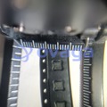
Paket/Gehäuse: SOP-8
Produktart: Power Driver ICs
RoHS-Status:
Lagerzustand: 90 Stück, Neues Original
Warranty: 1 Year Ovaga Warranty - Find Out More
0
1
BOMUCC27211DDAR Allgemeine Beschreibung
The UCC27210 and UCC27211 drivers are based on the popular UCC27200 and UCC27201 MOSFET drivers, but offer several significant performance improvements. Peak output pull-up and pull-down current has been increased to 4-A source and 4-A sink, and pull-up and pull-down resistance have been reduced to 0.9 Ω, thereby allowing for driving large power MOSFETs with minimized switching losses during the transition through the Miller Plateau of the MOSFET. The input structure is now able to directly handle 10 VDC, which increases robustness and also allows direct interface to gate-drive transformers without using rectification diodes. The inputs are also independent of supply voltage and have a maximum rating of 20-V.
The switching node (HS pin) of the UCC2721x can handle 18 V maximum which allows the high-side channel to be protected from inherent negative voltages caused parasitic inductance and stray capacitance. The UCC27210 (Pseudo-CMOS inputs) and UCC27211 (TTL inputs) have increased hysteresis allowing for interface to analog or digital PWM controllers with enhanced noise immunity.
The low-side and high-side gate drivers are independently controlled and matched to 2 ns between the turnon and turnoff of each other.
An on-chip 120-V rated bootstrap diode eliminates the external discrete diodes. Undervoltage lockout is provided for both the high-side and the low-side drivers providing symmetric turnon and turnoff behavior and forcing the outputs low if the drive voltage is below the specified threshold.
Both devices are offered in 8-pin SOIC (D), PowerPAD SOIC-8 (DDA), 4-mm × 4-mm SON-8 (DRM) and SON-10 (DPR) packages.
Funktionen
- Drives Two N-Channel MOSFETs in High-Side
and Low-Side Configuration With Independent
Inputs - Maximum Boot Voltage 120-V DC
- 4-A Sink, 4-A Source Output Currents
- 0.9-Ω Pullup and Pulldown Resistance
- Input Pins Can Tolerate –10 V to 20 V and Are
Independent of Supply Voltage Range - TTL or Pseudo-CMOS Compatible Input Versions
- 8-V to 17-V VDD Operating Range, (20-V Absolute
Maximum) - 7.2-ns Rise and 5.5-ns Fall Time With 1000-pF
Load - Fast Propagation Delay Times (18 ns Typical)
- 2-ns Delay Matching
- Symmetrical Undervoltage Lockout for High-Side
and Low-Side Driver - All Industry Standard Packages Available (SOIC-8,
PowerPAD™ SOIC-8, 4-mm × 4-mm SON-8
and 4-mm × 4-mm SON-10) - Specified from –40 to 140 °C
Spezifikationen
| Parameter | Wert | Parameter | Wert |
|---|---|---|---|
| Bus voltage (max) (V) | 110 | Power switch | MOSFET |
| Input VCC (min) (V) | 8 | Input VCC (max) (V) | 17 |
| Peak output current (A) | 4 | Operating temperature range (°C) | -40 to 140 |
| Undervoltage lockout (typ) (V) | 8 | Rating | Catalog |
| Propagation delay time (µs) | 0.02 | Rise time (ns) | 8 |
| Fall time (ns) | 7 | Iq (mA) | 0.001 |
| Input threshold | TTL | Channel input logic | TTL |
| Negative voltage handling at HS pin (V) | -12 |
Versand
| Versandart | Versandgebühr | Vorlaufzeit | |
|---|---|---|---|
 |
DHL | $20.00-$40.00 (0.50 KG) | 2-5 Tage |
 |
FedEx | $20.00-$40.00 (0.50 KG) | 2-5 Tage |
 |
UPS | $20.00-$40.00 (0.50 KG) | 2-5 Tage |
 |
TNT | $20.00-$40.00 (0.50 KG) | 2-5 Tage |
 |
EMS | $20.00-$40.00 (0.50 KG) | 2-5 Tage |
 |
REGISTRIERTE LUFTPOST | $20.00-$40.00 (0.50 KG) | 2-5 Tage |
Bearbeitungszeit: Die Versandkosten hängen von der jeweiligen Zone und dem Land ab.
Zahlung
| Zahlungsbedingungen | Handgebühr | |
|---|---|---|
 |
Banküberweisung | Bankgebühr in Höhe von 30,00 USD wird berechnet. |
 |
Paypal | 4,0 % Servicegebühr wird berechnet. |
 |
Kreditkarte | 3,5 % Servicegebühr wird berechnet. |
 |
Western Union | charge US.00 banking fee. |
 |
Geldgramm | Bankgebühr in Höhe von 0,00 USD wird berechnet. |
Garantien
1. Die von Ihnen gekauften elektronischen Bauteile enthalten eine 365-tägige Garantie. Wir garantieren die Produktqualität.
2. Wenn einige der Artikel, die Sie erhalten haben, nicht von perfekter Qualität sind, würden wir verantwortungsvoll Ihre Rückerstattung oder Ersatz arrangieren. Die Artikel müssen jedoch in ihrem Originalzustand verbleiben.
Verpackung
-

Schritt1 :Produkt
-

Schritt2 :Vakuumverpackung
-

Schritt3 :Antistatikbeutel
-

Schritt4 :Individuelle Verpackung
-

Schritt5 :Verpackungskartons
-

Schritt6 :Barcode-Versandetikett


Alle Produkte werden in antistatischen Beuteln verpackt. Versand mit ESD-Antistatikschutz.
Auf dem äußeren ESD-Verpackungsetikett werden die Informationen unseres Unternehmens verwendet: Teilenummer, Marke und Menge.
Wir prüfen alle Waren vor dem Versand, stellen sicher, dass sich alle Produkte in gutem Zustand befinden und dass die Teile neu und original sind und mit dem Datenblatt übereinstimmen.
Nachdem alle Waren darauf überprüft wurden, dass nach dem Verpacken keine Probleme auftreten, werden wir sicher verpacken und per Global Express versenden. Es zeigt eine ausgezeichnete Durchstoß- und Reißfestigkeit sowie eine gute Dichtungsintegrität.


Teilpunkte
-
The UCC27211DDAR chip is a dual-channel, high-speed gate driver designed for driving power MOSFETs in applications such as motor control, power supplies, and lighting. It offers robust protection features and excellent performance, making it ideal for high-power applications requiring fast switching speeds and precise control.
-
Equivalent
The equivalent products of UCC27211DDAR chip are UCC27211, UCC27212, UCC27213, and UCC27214. These chips are part of the UCC27211 family of high-speed, gate drivers with 4 A source and 4 A sink current capability. They are designed for driving power MOSFETs and IGBTs in half-bridge and full-bridge configurations. -
Features
1. Dual 4-A/8-A peak source/sink output current 2. Supports up to 60-V input voltage 3. Integrated bootstrap diode 4. Programmable dead time control 5. Adaptive shoot-through protection 6. Integrated undervoltage lockout and thermal shutdown 7. 5-V regulator with 10-mA output 8. Adjustable soft-start 9. Supports up to 2.2-MHz switching frequency -
Pinout
The UCC27211DDAR has 8 pins and functions as a high-speed, dual MOSFET driver with 4-A peak source and sink current capabilities. It is commonly used in high-side and low-side driver applications, such as synchronous buck converters and half-bridge inverters. -
Manufacturer
The UCC27211DDAR is manufactured by Texas Instruments, a leading semiconductor company that produces a wide range of integrated circuits and embedded processors for various industries including automotive, industrial, and consumer electronics. Texas Instruments is known for its high-quality products and innovative solutions in the field of analog and digital technologies. -
Application Field
The UCC27211DDAR is commonly used in high-side or low-side gate driver applications for power MOSFETs and IGBTs. It finds applications in power supplies, motor drives, and inverter systems for industrial and automotive sectors. Its features like high output current, low propagation delay, and high common-mode rejection ratio make it suitable for fast switching and high efficiency systems. -
Package
The UCC27211DDAR chip comes in a standard surface mount package type known as SOIC-8. It is a dual-channel low side gate driver with a form factor of an integrated circuit (IC) and a standardized size of 8 pins.


Wir bieten qualitativ hochwertige Produkte, durchdachten Service und eine Kundendienstgarantie
-

Wir haben reichhaltige Produkte, die Ihre unterschiedlichen Bedürfnisse erfüllen können.
-

Die Mindestbestellmenge beginnt bei 1 Stück.
-

Niedrigste internationale Versandgebühr beginnt ab 0,00 USD
-

365 Tage Qualitätsgarantie für alle Produkte