


Bilder dienen nur zur Referenz. Siehe Produktspezifikationen.
Bestellungen über
$5000NXP MC9S12DG256
Versatile digital signal processor for real-time data processing


Marken: NXP
Herstellerteil #: MC9S12DG256
Datenblatt: MC9S12DG256 Datenblatt (PDF)
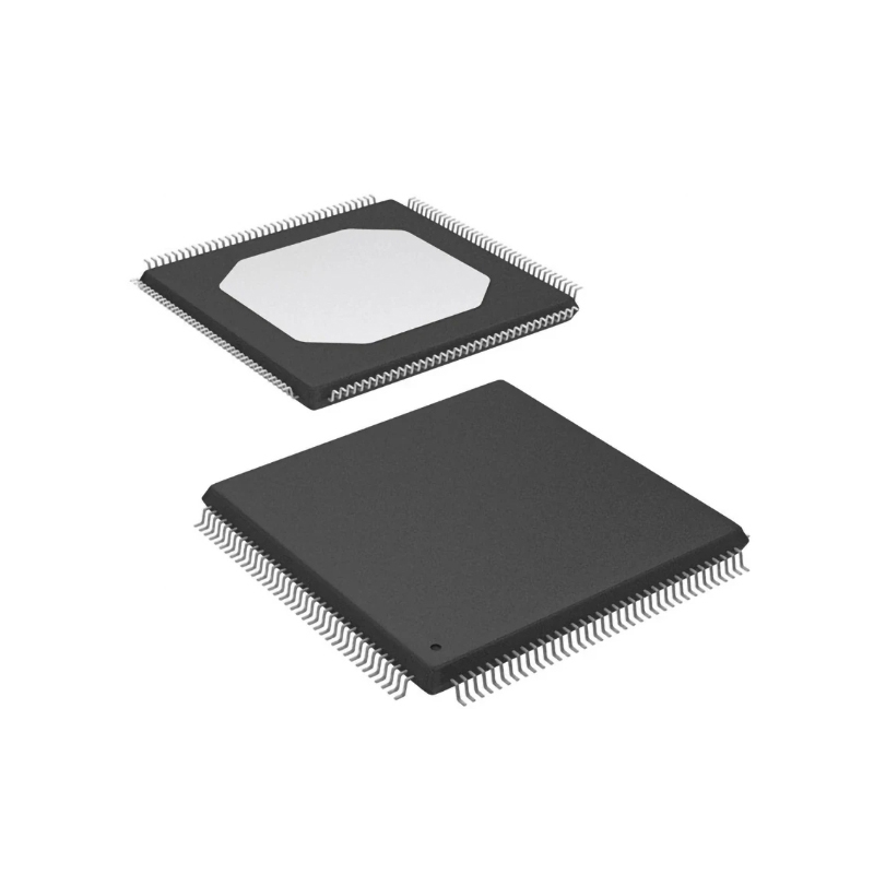
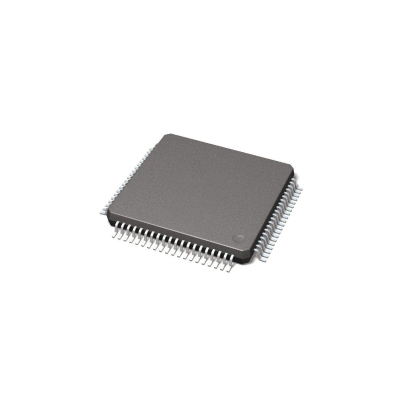
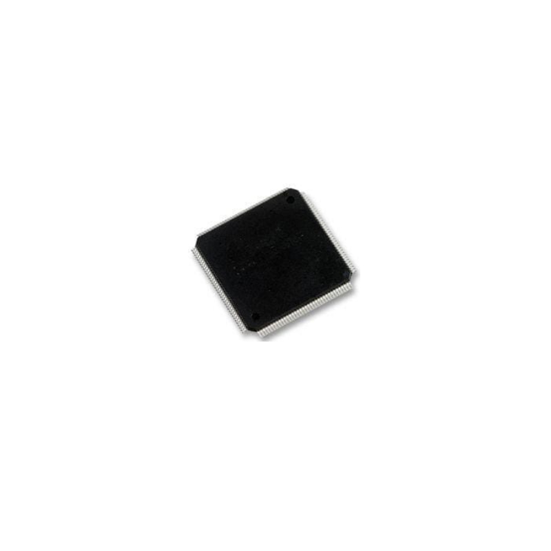
Paket/Gehäuse: QFP
Produktart: Single FETs, MOSFETs
RoHS-Status:
Lagerzustand: 6.554 Stück, Neues Original
Warranty: 1 Year Ovaga Warranty - Find Out More
0
1
MC9S12DG256 Allgemeine Beschreibung
OverviewThe MC9S12DT256 microcontroller unit (MCU) is a 16-bit device composed of standard on-chip peripherals including a 16-bit central processing unit (HCS12 CPU), 256K bytes of Flash EEPROM, 12K bytes of RAM, 4K bytes of EEPROM, two asynchronous serial communications interfaces (SCI), three serial peripheral interfaces (SPI), an 8-channel IC/OC enhanced capture timer, two 8-channel, 10-bit analog-to-digital converters (ADC), an 8-channel pulse-width modulator (PWM), a digital Byte Data Link Controller (BDLC), 29 discrete digital I/O channels (Port A, Port B, Port K and Port E), 20 discrete digital I/O lines with interrupt and wakeup capability, three CAN 2.0 A, B software compatible modules (MSCAN12), and an Inter-IC Bus. The MC9S12DT256 has full 16-bit data paths throughout. However, the external bus can operate in an 8-bit narrow mode so single 8-bit wide memory can be interfaced for lower cost systems. The inclusion of a PLL circuit allows power consumption and performance to be adjusted to suit operational requirements.Features• HCS12 Core – 16-bit HCS12 CPU i. Upward compatible with M68HC11 instruction set ii. Interrupt stacking and programmer’s model identical to M68HC11 iii.Instruction queue iv. Enhanced indexed addressing – MEBI (Multiplexed External Bus Interface) – MMC (Module Mapping Control) – INT (Interrupt control) – BKP (Breakpoints) – BDM (Background Debug Mode)• CRG – Low current Colpitts or Pierce oscillator – PLL – COP watchdog – Real time interrupt – Clock Monitor• 8-bit and 4-bit ports with interrupt functionality – Digital filtering – Programmable rising or falling edge trigger• Memory – 256K Flash EEPROM – 4K byte EEPROM – 12K byte RAM• Two 8-channel Analog-to-Digital Converters – 10-bit resolution – External conversion trigger capability• Three 1M bit per second, CAN 2.0 A, B software compatible modules – Five receive and three transmit buffers – Flexible identifier filter programmable as 2 x 32 bit, 4 x 16 bit or 8 x 8 bit – Four separate interrupt channels for Rx, Tx, error and wake-up – Low-pass filter wake-up function – Loop-back for self test operation• Enhanced Capture Timer – 16-bit main counter with 7-bit prescaler – 8 programmable input capture or output compare channels – Four 8-bit or two 16-bit pulse accumulators• 8 PWM channels – Programmable period and duty cycle – 8-bit 8-channel or 16-bit 4-channel – Separate control for each pulse width and duty cycle – Center-aligned or left-aligned outputs – Programmable clock select logic with a wide range of frequencies – Fast emergency shutdown input – Usable as interrupt inputs• Serial interfaces – Two asynchronous Serial Communications Interfaces (SCI) – Three Synchronous Serial Peripheral Interface (SPI)• Byte Data Link Controller (BDLC) – SAE J1850 Class B Data Communications Network Interface Compatible and ISO Compatible for Low-Speed (<125 Kbps) Serial Data Communications in Automotive Applications• Inter-IC Bus (IIC) – Compatible with I2C Bus standard – Multi-master operation – Software programmable for one of 256 different serial clock frequencies• 112-Pin LQFP package – I/O lines with 5V input and drive capability – 5V A/D converter inputs – Operation at 50MHz equivalent to 25MHz Bus Speed – Development support – Single-wire background debug™ mode (BDM) – On-chip hardware breakpoints
Funktionen
- HCS12 Core
- – 16-bit HCS12 CPU
- i. Upward compatible with M68HC11 instruction set
- ii. Interrupt stacking and programmer’s model identical to M68HC11
- iii.Instruction queue
- iv. Enhanced indexed addressing
- – MEBI (Multiplexed External Bus Interface)
- – MMC (Module Mapping Control)
- – INT (Interrupt control)
- – BKP (Breakpoints)
- – BDM (Background Debug Mode)
- CRG
- – Low current Colpitts or Pierce oscillator
- – PLL
- – COP watchdog
- – Real time interrupt
- – Clock Monitor
- 8-bit and 4-bit ports with interrupt functionality
- – Digital filtering
- – Programmable rising or falling edge trigger
- Memory
- – 256K Flash EEPROM
- – 4K byte EEPROM
- – 12K byte RAM
- Two 8-channel Analog-to-Digital Converters
- – 10-bit resolution
- – External conversion trigger capability
- Three 1M bit per second, CAN 2.0 A, B software compatible modules
- – Five receive and three transmit buffers
- – Flexible identifier filter programmable as 2 x 32 bit, 4 x 16 bit or 8 x 8 bit
- – Four separate interrupt channels for Rx, Tx, error and wake-up
- – Low-pass filter wake-up function
- – Loop-back for self test operation
- Enhanced Capture Timer
- – 16-bit main counter with 7-bit prescaler
- – 8 programmable input capture or output compare channels
- – Four 8-bit or two 16-bit pulse accumulators
- 8 PWM channels
- – Programmable period and duty cycle
- – 8-bit 8-channel or 16-bit 4-channel
- – Separate control for each pulse width and duty cycle
- – Center-aligned or left-aligned outputs
- – Programmable clock select logic with a wide range of frequencies
- – Fast emergency shutdown input
- – Usable as interrupt inputs
- Serial interfaces
- – Two asynchronous Serial Communications Interfaces (SCI)
- – Three Synchronous Serial Peripheral Interface (SPI)
- Byte Data Link Controller (BDLC)
- – SAE J1850 Class B Data Communications Network Interface Compatible and ISO Compatible for Low-Speed (<125 Kbps) Serial Data Communications in Automotive Applications
- Inter-IC Bus (IIC)
- – Compatible with I2C Bus standard
- – Multi-master operation
- – Software programmable for one of 256 different serial clock frequencies
- 112-Pin LQFP package
- – I/O lines with 5V input and drive capability
- – 5V A/D converter inputs
- – Operation at 50MHz equivalent to 25MHz Bus Speed
- – Development support
- – Single-wire background debug™ mode (BDM)
- – On-chip hardware breakpoints
Anwendung
- The MC9S12DG256 is commonly used in various applications, including:
- Automotive systems, such as engine control units, body control modules, and instrument clusters
- Industrial control systems, such as motor control, robotics, and automation
- Consumer electronics, including home appliances, gaming devices, and multimedia systems
- Communication devices, such as routers, modems, and gateways
- Medical devices, such as patient monitors and diagnostic equipment
Spezifikationen
| Parameter | Wert | Parameter | Wert |
|---|---|---|---|
| Product Name | MC9S12DG256 | Product Type | Microcontroller |
| Manufacturer | NXP Semiconductors | Series | MC9S12 |
| Core Processor | HCS12 | Core Size | 16-Bit |
| Speed | 40MHz | Connectivity | CAN, LIN, SPI, UART/USART |
| Peripherals | ADC, PWM, Timer/Counter, Watchdog Timer | Number of I/Os | 112 |
| Program Memory Size | 256KB | Data RAM Size | 8KB |
| Voltage - Supply | 2.35 V ~ 5.5 V | Operating Temperature | -40°C ~ 125°C |
| Mounting Type | Surface Mount |
Versand
| Versandart | Versandgebühr | Vorlaufzeit | |
|---|---|---|---|
 |
DHL | $20.00-$40.00 (0.50 KG) | 2-5 Tage |
 |
FedEx | $20.00-$40.00 (0.50 KG) | 2-5 Tage |
 |
UPS | $20.00-$40.00 (0.50 KG) | 2-5 Tage |
 |
TNT | $20.00-$40.00 (0.50 KG) | 2-5 Tage |
 |
EMS | $20.00-$40.00 (0.50 KG) | 2-5 Tage |
 |
REGISTRIERTE LUFTPOST | $20.00-$40.00 (0.50 KG) | 2-5 Tage |
Bearbeitungszeit: Die Versandkosten hängen von der jeweiligen Zone und dem Land ab.
Zahlung
| Zahlungsbedingungen | Handgebühr | |
|---|---|---|
 |
Banküberweisung | Bankgebühr in Höhe von 30,00 USD wird berechnet. |
 |
Paypal | 4,0 % Servicegebühr wird berechnet. |
 |
Kreditkarte | 3,5 % Servicegebühr wird berechnet. |
 |
Western Union | charge US.00 banking fee. |
 |
Geldgramm | Bankgebühr in Höhe von 0,00 USD wird berechnet. |
Garantien
1. Die von Ihnen gekauften elektronischen Bauteile enthalten eine 365-tägige Garantie. Wir garantieren die Produktqualität.
2. Wenn einige der Artikel, die Sie erhalten haben, nicht von perfekter Qualität sind, würden wir verantwortungsvoll Ihre Rückerstattung oder Ersatz arrangieren. Die Artikel müssen jedoch in ihrem Originalzustand verbleiben.
Verpackung
-

Schritt1 :Produkt
-

Schritt2 :Vakuumverpackung
-

Schritt3 :Antistatikbeutel
-

Schritt4 :Individuelle Verpackung
-

Schritt5 :Verpackungskartons
-

Schritt6 :Barcode-Versandetikett


Alle Produkte werden in antistatischen Beuteln verpackt. Versand mit ESD-Antistatikschutz.
Auf dem äußeren ESD-Verpackungsetikett werden die Informationen unseres Unternehmens verwendet: Teilenummer, Marke und Menge.
Wir prüfen alle Waren vor dem Versand, stellen sicher, dass sich alle Produkte in gutem Zustand befinden und dass die Teile neu und original sind und mit dem Datenblatt übereinstimmen.
Nachdem alle Waren darauf überprüft wurden, dass nach dem Verpacken keine Probleme auftreten, werden wir sicher verpacken und per Global Express versenden. Es zeigt eine ausgezeichnete Durchstoß- und Reißfestigkeit sowie eine gute Dichtungsintegrität.


Äquivalente Teile
Für den MC9S12DG256 Komponente, Sie könnten diese Ersatz- und Alternativteile in Betracht ziehen:
Artikelnummer
Marken
Paket
Beschreibung
Artikelnummer : MC9S12DG256
Marken :
Paket : QFP
Beschreibung : The MC9S12DG256 does not have a direct equivalent part number from other manufacturers, as it is a specific MCU from NXP Semiconductors. However, there are other microcontrollers available in the market with similar features and capabilities, such as the STM32F407 from STMicroelectronics and the PIC32MX795F512L from Microchip.

Wir bieten qualitativ hochwertige Produkte, durchdachten Service und eine Kundendienstgarantie
-

Wir haben reichhaltige Produkte, die Ihre unterschiedlichen Bedürfnisse erfüllen können.
-

Die Mindestbestellmenge beginnt bei 1 Stück.
-

Niedrigste internationale Versandgebühr beginnt ab 0,00 USD
-

365 Tage Qualitätsgarantie für alle Produkte


