


Bilder dienen nur zur Referenz. Siehe Produktspezifikationen.
Bestellungen über
$5000
ON MUN5315DW1T1G

Trans Digital BJT NPN/PNP: MUN5315DW1T1G, 50V, 100mA, 6-Pin SOT-363, Tape and Reel


Marken: Onsemi
Herstellerteil #: MUN5315DW1T1G
Datenblatt: MUN5315DW1T1G Datasheet (PDF)
Paket/Gehäuse: SC-88-6
RoHS-Status:
Lagerzustand: 2.526 Stück, Neues Original
Produktart: Bipolar Transistor Arrays, Pre-Biased
Warranty: 1 Year Ovaga Warranty - Find Out More
0
1
*Alle Preise sind in USD
| Menge | Einzelpreis | Ext. Preis |
|---|---|---|
| 1 | $0,095 | $0,095 |
| 200 | $0,037 | $7,400 |
| 500 | $0,036 | $18,000 |
| 1000 | $0,035 | $35,000 |
Auf Lager: 2.526 Stck
MUN5315DW1T1G Allgemeine Beschreibung
ON Semiconductor's MUN5315DW1T1G stands out as a dual N-channel MOSFET transistor designed to meet the needs of general-purpose switching applications. It boasts a 30V drain-to-source voltage rating and a 3.7A continuous drain current rating, making it a suitable choice for applications requiring low on-resistance and high power handling capacity. Furthermore, its low gate threshold voltage of 1.5V and low on-resistance of 0.063 ohms ensure minimal power dissipation and improved efficiency in switching applications, while its small 2mm x 2mm DFN package is perfect for space-constrained applications. With a maximum operating temperature of 150°C, this dual MOSFET provides reliable performance across a wide range of operating conditions
Funktionen
- MOSFET MUN53 offers 60V operation and 48A continuous drain current
- It has an on-resistance of just 21mOhm, reducing power losses
Anwendung
- GaN transistor for high-power apps
- Military, radar, satellite use
- Efficient and reliable performance
Spezifikationen
| Parameter | Wert | Parameter | Wert |
|---|---|---|---|
| Product Category | Digital Transistors | RoHS | Details |
| Configuration | Dual | Transistor Polarity | NPN, PNP |
| Typical Input Resistor | 10 kOhms | Mounting Style | SMD/SMT |
| Package / Case | SC-88-6 | DC Collector/Base Gain hfe Min | 160 |
| Collector- Emitter Voltage VCEO Max | 50 V | Continuous Collector Current | 100 mA |
| Peak DC Collector Current | 100 mA | Pd - Power Dissipation | 187 mW |
| Minimum Operating Temperature | - 55 C | Maximum Operating Temperature | + 150 C |
| Series | MUN5315DW1 | Brand | onsemi |
| DC Current Gain hFE Max | 160 at 5 mA at 10 V | Height | 0.9 mm |
| Length | 2 mm | Number of Channels | 2 Channel |
| Product Type | Digital Transistors | Factory Pack Quantity | 3000 |
| Subcategory | Transistors | Width | 1.25 mm |
| Unit Weight | 0.000219 oz |
Versand
| Versandart | Versandgebühr | Vorlaufzeit | |
|---|---|---|---|
 |
DHL | $20.00-$40.00 (0.50 KG) | 2-5 Tage |
 |
FedEx | $20.00-$40.00 (0.50 KG) | 2-5 Tage |
 |
UPS | $20.00-$40.00 (0.50 KG) | 2-5 Tage |
 |
TNT | $20.00-$40.00 (0.50 KG) | 2-5 Tage |
 |
EMS | $20.00-$40.00 (0.50 KG) | 2-5 Tage |
 |
REGISTRIERTE LUFTPOST | $20.00-$40.00 (0.50 KG) | 2-5 Tage |
Bearbeitungszeit: Die Versandkosten hängen von der jeweiligen Zone und dem Land ab.
Zahlung
| Zahlungsbedingungen | Handgebühr | |
|---|---|---|
 |
Banküberweisung | Bankgebühr in Höhe von 30,00 USD wird berechnet. |
 |
Paypal | 4,0 % Servicegebühr wird berechnet. |
 |
Kreditkarte | 3,5 % Servicegebühr wird berechnet. |
 |
Western Union | charge US.00 banking fee. |
 |
Geldgramm | Bankgebühr in Höhe von 0,00 USD wird berechnet. |
Garantien
1. Die von Ihnen gekauften elektronischen Bauteile enthalten eine 365-tägige Garantie. Wir garantieren die Produktqualität.
2. Wenn einige der Artikel, die Sie erhalten haben, nicht von perfekter Qualität sind, würden wir verantwortungsvoll Ihre Rückerstattung oder Ersatz arrangieren. Die Artikel müssen jedoch in ihrem Originalzustand verbleiben.
Verpackung
-

Schritt1 :Produkt
-

Schritt2 :Vakuumverpackung
-

Schritt3 :Antistatikbeutel
-

Schritt4 :Individuelle Verpackung
-

Schritt5 :Verpackungskartons
-

Schritt6 :Barcode-Versandetikett


Alle Produkte werden in antistatischen Beuteln verpackt. Versand mit ESD-Antistatikschutz.
Auf dem äußeren ESD-Verpackungsetikett werden die Informationen unseres Unternehmens verwendet: Teilenummer, Marke und Menge.
Wir prüfen alle Waren vor dem Versand, stellen sicher, dass sich alle Produkte in gutem Zustand befinden und dass die Teile neu und original sind und mit dem Datenblatt übereinstimmen.
Nachdem alle Waren darauf überprüft wurden, dass nach dem Verpacken keine Probleme auftreten, werden wir sicher verpacken und per Global Express versenden. Es zeigt eine ausgezeichnete Durchstoß- und Reißfestigkeit sowie eine gute Dichtungsintegrität.


Teilpunkte
-
The MUN5315DW1T1G chip is an NPN lownoise amplifier transistor designed for applications in wireless communication systems. It operates in the frequency range of 900MHz to 2GHz and offers a low noise figure of 1.1dB, making it suitable for sensitive signal amplification. The chip is housed in a small SOT-323 package, which enables compact designs for space-constrained applications.
-
Features
The MUN5315DW1T1G is a NPN Bipolar Power Transistor with a high collector current capability of 5A, low saturation voltage, and fast switching speed. It is designed for general-purpose amplifier and switching applications in power supply systems, motor control, and consumer electronics. -
Pinout
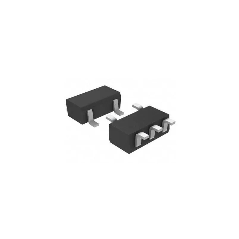
The MUN5315DW1T1G is a dual NPN/PNP bipolar transistor with 6 pins. The first 3 pins are for connection to the NPN transistor, and the last 3 pins are for connection to the PNP transistor. The device is designed for switching applications in automotive and general-purpose use. -
Manufacturer
The manufacturer of the MUN5315DW1T1G is ON Semiconductor. It is a multinational semiconductor supplier company. -
Application Field
The MUN5315DW1T1G is an NPN bipolar transistor commonly used in a variety of applications, including switching and amplification circuits, power management systems, and in various electronic devices requiring high voltage and current capabilities. -
Package
The MUN5315DW1T1G chip is available in a SOT-363 package, which is a small surface-mount package. The chip has a form factor of a small rectangular shape with four terminals. The overall package size is approximately 2.0mm x 1.25mm x 0.75mm.


Datenblatt PDF
Wir bieten qualitativ hochwertige Produkte, durchdachten Service und eine Kundendienstgarantie
-

Wir haben reichhaltige Produkte, die Ihre unterschiedlichen Bedürfnisse erfüllen können.
-

Die Mindestbestellmenge beginnt bei 1 Stück.
-

Niedrigste internationale Versandgebühr beginnt ab 0,00 USD
-

365 Tage Qualitätsgarantie für alle Produkte


