

Bilder dienen nur zur Referenz. Siehe Produktspezifikationen.
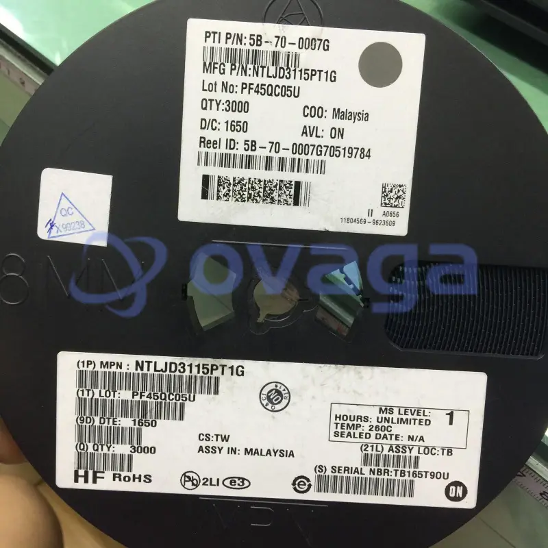
ON NTLJD3115PT1G
Mosfet Array 20V 2.3A 710mW Surface Mount 6-WDFN (2x2)


Marken: ON Semiconductor, LLC
Herstellerteil #: NTLJD3115PT1G
Datenblatt: NTLJD3115PT1G Datasheet (PDF)
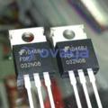
Paket/Gehäuse: WDFN EP
Produktart: Transistoren
RoHS-Status:
Lagerzustand: 3602 Stück, Neues Original
Warranty: 1 Year Ovaga Warranty - Find Out More
0
1
BOMNTLJD3115PT1G Allgemeine Beschreibung
Mosfet Array 20V 2.3A 710mW Surface Mount 6-WDFN (2x2)
Funktionen
- WDFN Package Provides Exposed Drain Pad for Excellent Thermal Conduction
- 2x2 mm Footprint Same as SC-88
- Lowest RDS(on) Solution in 2x2 mm Package
- 1.8 V RDS(on) Rating for Operation at Low Voltage Gate Drive Logic Level
- Low Profile (< 0.8 mm) for Easy Fit in Thin Environments
- Bidirectional Current Flow with Common Source Configuration
Anwendung
- Optimized for Battery and Load Management Applications in Portable Equipment
- Li-Ion Battery Charging and Protection Circuits
- High Side Load Switch
Spezifikationen
| Parameter | Wert | Parameter | Wert |
|---|---|---|---|
| Source Content uid | NTLJD3115PT1G | Pbfree Code | Yes |
| Part Life Cycle Code | Active | Ihs Manufacturer | ONSEMI |
| Part Package Code | WDFN6 2x2, 0.65P | Package Description | WDFN-6 |
| Pin Count | 6 | Manufacturer Package Code | 506AN |
| Reach Compliance Code | compliant | ECCN Code | EAR99 |
| Factory Lead Time | 22 Weeks | Samacsys Manufacturer | onsemi |
| Additional Feature | LOGIC LEVEL COMPATIBLE | Case Connection | DRAIN |
| Configuration | SEPARATE, 2 ELEMENTS WITH BUILT-IN DIODE | DS Breakdown Voltage-Min | 20 V |
| Drain Current-Max (ID) | 2.3 A | Drain-source On Resistance-Max | 0.135 Ω |
| FET Technology | METAL-OXIDE SEMICONDUCTOR | JESD-30 Code | S-PDSO-N6 |
| JESD-609 Code | e3 | Moisture Sensitivity Level | 1 |
| Number of Elements | 1 | Number of Terminals | 6 |
| Operating Mode | ENHANCEMENT MODE | Operating Temperature-Max | 150 °C |
| Operating Temperature-Min | -55 °C | Package Body Material | PLASTIC/EPOXY |
| Package Shape | RECTANGULAR | Package Style | SMALL OUTLINE |
| Peak Reflow Temperature (Cel) | 260 | Polarity/Channel Type | P-CHANNEL |
| Power Dissipation-Max (Abs) | 1.5 W | Pulsed Drain Current-Max (IDM) | 20 A |
| Qualification Status | Not Qualified | Surface Mount | YES |
| Terminal Finish | MATTE TIN | Terminal Form | NO LEAD |
| Terminal Position | DUAL | Time@Peak Reflow Temperature-Max (s) | 30 |
| Transistor Application | SWITCHING | Transistor Element Material | SILICON |
| feature-category | Power MOSFET | feature-material | |
| feature-process-technology | feature-configuration | Dual | |
| feature-channel-mode | Enhancement | feature-channel-type | P |
| feature-number-of-elements-per-chip | 2 | feature-maximum-drain-source-voltage-v | 20 |
| feature-maximum-gate-source-voltage-v | ±8 | feature-maximum-gate-threshold-voltage-v | 1 |
| feature-maximum-continuous-drain-current-a | 3.3 | feature-maximum-drain-source-resistance-mohm | [email protected] |
| feature-typical-gate-charge-vgs-nc | [email protected] | feature-typical-gate-charge-10v-nc | 5.5 |
| feature-typical-input-capacitance-vds-pf | 531@10V | feature-typical-output-capacitance-pf | 91 |
| feature-maximum-power-dissipation-mw | 2300 | feature-packaging | Tape and Reel |
| feature-rad-hard | feature-pin-count | 6 | |
| feature-supplier-package | WDFN EP | feature-standard-package-name1 | DFN |
| feature-cecc-qualified | No | feature-esd-protection | |
| feature-military | No | feature-aec-qualified | No |
| feature-aec-qualified-number | feature-auto-motive | No | |
| feature-p-pap | No | feature-eccn-code | EAR99 |
| feature-svhc | No |
Versand
| Versandart | Versandgebühr | Vorlaufzeit | |
|---|---|---|---|
 |
DHL | $20.00-$40.00 (0.50 KG) | 2-5 Tage |
 |
FedEx | $20.00-$40.00 (0.50 KG) | 2-5 Tage |
 |
UPS | $20.00-$40.00 (0.50 KG) | 2-5 Tage |
 |
TNT | $20.00-$40.00 (0.50 KG) | 2-5 Tage |
 |
EMS | $20.00-$40.00 (0.50 KG) | 2-5 Tage |
 |
REGISTRIERTE LUFTPOST | $20.00-$40.00 (0.50 KG) | 2-5 Tage |
Bearbeitungszeit: Die Versandkosten hängen von der jeweiligen Zone und dem Land ab.
Zahlung
| Zahlungsbedingungen | Handgebühr | |
|---|---|---|
 |
Banküberweisung | Bankgebühr in Höhe von 30,00 USD wird berechnet. |
 |
Paypal | 4,0 % Servicegebühr wird berechnet. |
 |
Kreditkarte | 3,5 % Servicegebühr wird berechnet. |
 |
Western Union | charge US.00 banking fee. |
 |
Geldgramm | Bankgebühr in Höhe von 0,00 USD wird berechnet. |
Garantien
1. Die von Ihnen gekauften elektronischen Bauteile enthalten eine 365-tägige Garantie. Wir garantieren die Produktqualität.
2. Wenn einige der Artikel, die Sie erhalten haben, nicht von perfekter Qualität sind, würden wir verantwortungsvoll Ihre Rückerstattung oder Ersatz arrangieren. Die Artikel müssen jedoch in ihrem Originalzustand verbleiben.
Verpackung
-

Schritt1 :Produkt
-

Schritt2 :Vakuumverpackung
-

Schritt3 :Antistatikbeutel
-

Schritt4 :Individuelle Verpackung
-

Schritt5 :Verpackungskartons
-

Schritt6 :Barcode-Versandetikett


Alle Produkte werden in antistatischen Beuteln verpackt. Versand mit ESD-Antistatikschutz.
Auf dem äußeren ESD-Verpackungsetikett werden die Informationen unseres Unternehmens verwendet: Teilenummer, Marke und Menge.
Wir prüfen alle Waren vor dem Versand, stellen sicher, dass sich alle Produkte in gutem Zustand befinden und dass die Teile neu und original sind und mit dem Datenblatt übereinstimmen.
Nachdem alle Waren darauf überprüft wurden, dass nach dem Verpacken keine Probleme auftreten, werden wir sicher verpacken und per Global Express versenden. Es zeigt eine ausgezeichnete Durchstoß- und Reißfestigkeit sowie eine gute Dichtungsintegrität.


Teilpunkte
-
The NTLJD3115PT1G chip is a high-speed, low voltage dual N-channel MOSFET designed for applications such as load and motor control. It has a compact 2mm x 2mm package and features low on-resistance with fast switching capabilities. This chip is suitable for use in a variety of electronic devices that require efficient power management and control.
-
Features
The NTLJD3115PT1G is a high-performance N-channel MOSFET transistor. It has a low on-resistance, high power dissipation capability, and is designed for applications requiring high efficiency power conversion. The device offers low gate charge which enables faster switching, making it suitable for various applications including power supplies, motor controls, and automotive systems. -
Pinout
The NTLJD3115PT1G is a MOSFET transistor with a 6-pin DFN package. It is a dual N-Channel enhancement mode transistor designed for low voltage, high-speed switching applications. The pin count includes 3 pins per channel: drain, source, and gate for each N-Channel. -
Manufacturer
The manufacturer of the NTLJD3115PT1G is ON Semiconductor. It is a semiconductor manufacturing company that specializes in designing and producing a wide range of integrated circuits, power management solutions, and discrete components for various industries including automotive, communications, consumer electronics, and industrial applications. -
Application Field
The NTLJD3115PT1G is a low on-resistance single-channel logic level N-channel MOSFET. It can be used in a variety of applications, including power management, load switching, battery charging, and motor control. Its compact package and high efficiency make it suitable for portable electronics, automotive systems, industrial equipment, and more. -
Package
The NTLJD3115PT1G chip is available in a surface mount package type known as SOT-563. It is a small form factor package with dimensions measuring approximately 1.6mm x 1.6mm x 0.6mm.


Datenblatt PDF
Wir bieten qualitativ hochwertige Produkte, durchdachten Service und eine Kundendienstgarantie
-

Wir haben reichhaltige Produkte, die Ihre unterschiedlichen Bedürfnisse erfüllen können.
-

Die Mindestbestellmenge beginnt bei 1 Stück.
-

Niedrigste internationale Versandgebühr beginnt ab 0,00 USD
-

365 Tage Qualitätsgarantie für alle Produkte


Shipping was prompt and efficient.